MM74C373N Fairchild Semiconductor, MM74C373N Datasheet

IC LATCH OCTAL D 3STATE 20-DIP

MM74C373N

Manufacturer Part Number
MM74C373N
Description
IC LATCH OCTAL D 3STATE 20-DIP
Manufacturer
Fairchild Semiconductor
Series
74Cr
Datasheet

Specifications of MM74C373N

Logic Type
D-Type Transparent Latch
Circuit
8:8
Output Type
Tri-State
Voltage - Supply
3 V ~ 15 V
Independent Circuits
1
Delay Time - Propagation
70ns
Current - Output High, Low
24mA, 24mA
Operating Temperature
-55°C ~ 125°C
Mounting Type
Through Hole
Package / Case
20-DIP (0.300", 7.62mm)
Number Of Circuits
8
Logic Family
74C
Polarity
Non-Inverting
High Level Output Current
- 48 mA
Propagation Delay Time
370 ns at 5 V, 170 ns at 10 V
Supply Voltage (max)
15 V
Supply Voltage (min)
3 V
Maximum Operating Temperature
+ 125 C
Minimum Operating Temperature
- 55 C
Mounting Style
Through Hole
Supply Current
0.3 mA
Latch Type
D Type
Output Current
48mA
Propagation Delay
85ns
No. Of Bits
8 Bit
Ic Output Type
Tri State
Supply Voltage Range
3V To 15V
Logic Case Style
DIP
No. Of Pins
20
Rohs Compliant
Yes
Lead Free Status / RoHS Status
Lead free / RoHS Compliant
Other names
74C373
74C373N

Available stocks

Company
Part Number
Manufacturer
Quantity
Price
Part Number:
MM74C373N
Manufacturer:
NS
Quantity:
7 464
© 2004 Fairchild Semiconductor Corporation
MM74C373M
(Note 1)
MM74C373N
MM74C374N
MM74C373 • MM74C374
3-STATE Octal D-Type Latch •
3-STATE Octal D-Type Flip-Flop
General Description
The MM74C373 and MM74C374 are integrated, comple-
mentary MOS (CMOS), 8-bit storage elements with 3-
STATE outputs. These outputs have been specially
designed to drive high capacitive loads, such as one might
find when driving a bus, and to have a fan out of 1 when
driving standard TTL. When a high logic level is applied to
the OUTPUT DISABLE input, all outputs go to a high
impedance state, regardless of what signals are present at
the other inputs and the state of the storage elements.
The MM74C373 is an 8-bit latch. When LATCH ENABLE is
high, the Q outputs will follow the D inputs. When LATCH
ENABLE goes low, data at the D inputs, which meets the
set-up and hold time requirements, will be retained at the
outputs until LATCH ENABLE returns high again.
The MM74C374 is an 8-bit, D-type, positive-edge triggered
flip-flop. Data at the D inputs, meeting the set-up and hold
time requirements, is transferred to the Q outputs on posi-
tive-going transitions of the CLOCK input.
Both the MM74C373 and the MM74C374 are being assem-
bled in 20-pin dual-in-line packages with 0.300” pin cen-
ters.
Ordering Code:
Note 1: Devices also available in Tape and Reel. Specify by appending the suffix letter “X” to the ordering code.
Order Number
Package Number
M20B
N20A
N20A
20-Lead Small Outline Integrated Circuit (SOIC), JEDEC MS-013, 0.300" Wide
20-Lead Plastic Dual-In-Line Package (PDIP), JEDEC MS-001, 0.300" Wide
DS005906
Features
Wide supply voltage range:
High noise immunity: 0.45 V
Low power consumption
TTL compatibility:
Bus driving capability
3-STATE outputs
Eight storage elements in one package
Single CLOCK/LATCH ENABLE and OUTPUT DIS-
ABLE control inputs
20-pin dual-in-line package with 0.300” centers takes
half the board space of a 24-pin package
Fan out of 1driving standard TTL
Package Description
October 1987
Revised January 2004
CC
3V to 15V
(typ.)
www.fairchildsemi.com

Related parts for MM74C373N

MM74C373N Summary of contents

Page 1

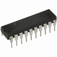
... Order Number Package Number MM74C373M M20B 20-Lead Small Outline Integrated Circuit (SOIC), JEDEC MS-013, 0.300" Wide (Note 1) MM74C373N N20A 20-Lead Plastic Dual-In-Line Package (PDIP), JEDEC MS-001, 0.300" Wide MM74C374N N20A 20-Lead Plastic Dual-In-Line Package (PDIP), JEDEC MS-001, 0.300" Wide Note 1: Devices also available in Tape and Reel. Specify by appending the suffix letter “X” to the ordering code. ...

Page 2

Connection Diagrams MM74C373 Top View Truth Tables MM74C373 Output LATCH D Disable ENABLE LOW logic level H HIGH logic level X Irrelevant www.fairchildsemi.com MM74C374 Top View MM74C374 ...

Page 3

Block Diagrams MM74C373 ( Latches) MM74C374 ( Flip-Flops) 3 www.fairchildsemi.com ...

Page 4

Absolute Maximum Ratings Voltage at Any Pin 0. Operating Temperature Range ( MM74C373 Storage Temperature Range ( Power Dissipation Dual-In-Line Small Outline Operating V Range CC Absolute Maximum V CC Lead Temperature (T ) ...

Page 5

AC Electrical Characteristics pF MM74C373 ns, unless otherwise noted Symbol Parameter Propagation Delay, pd0 pd1 LATCH ENABLE to Output Propagation Delay Data ...

Page 6

AC Electrical Characteristics pF MM74C374 ns, unless otherwise noted Symbol Parameter Propagation Delay, pd0 pd1 CLOCK to Output t Minimum Set-Up Time Data In SET-UP ...

Page 7

Typical Performance Characteristics MM74C373 Propagation Delay, LATCH ENABLE to Output vs Load Capacitance MM74C373 Propagation Delay, Data In to Output vs Load Capacitance MM74C373 Propagation Delay, CLOCK to Output vs Load Capacitance MM74C373, MM74C374 Change in Propagation Delay per pF ...

Page 8

Typical Applications Simple, Latching, Octal, LED Indicator Driver with Blanking for Use as Data Display, Bus Monitor, P Front Panel Display, Etc. 3-STATE Test Circuits and Switching Time Waveforms ...

Page 9

Switching Time Waveforms Output Disable GND Output Disable GND MM74C373 MM74C374 9 www.fairchildsemi.com ...

Page 10

Physical Dimensions inches (millimeters) unless otherwise noted 20-Lead Small Outline Integrated Circuit (SOIC), JEDEC MS-013, 0.300" Wide www.fairchildsemi.com Package Number M20B 10 ...

Page 11

Physical Dimensions inches (millimeters) unless otherwise noted (Continued) 20-Lead Plastic Dual-In-Line Package (PDIP), JEDEC MS-001, 0.300" Wide Fairchild does not assume any responsibility for use of any circuitry described, no circuit patent licenses are implied and Fairchild reserves the right ...

Related keywords