MC14044BDG ON Semiconductor, MC14044BDG Datasheet
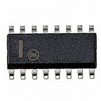
IC LATCH R-S QUAD P/N 16-SOIC

MC14044BDG

Manufacturer Part Number
MC14044BDG
Description
IC LATCH R-S QUAD P/N 16-SOIC
Manufacturer
ON Semiconductor
Series
4000Br
Datasheet

Specifications of MC14044BDG

Logic Type
S-R Latch
Circuit
1:1
Output Type
Tri-State
Voltage - Supply
3 V ~ 18 V
Independent Circuits
4
Delay Time - Propagation
60ns
Current - Output High, Low
8.8mA, 8.8mA
Operating Temperature
-55°C ~ 125°C
Mounting Type
Surface Mount
Package / Case
16-SOIC (3.9mm Width)
Number Of Circuits
4
Logic Family
MC14
Polarity
Non-Inverting
Input Bias Current (max)
0.006 uA
High Level Output Current
- 4.2 mA
Low Level Output Current
32 mA
Propagation Delay Time
350 ns at 5 V, 175 ns at 10 V, 120 ns at 15 V
Supply Voltage (max)
18 V
Supply Voltage (min)
3 V
Maximum Operating Temperature
+ 125 C
Minimum Operating Temperature
- 55 C
Mounting Style
SMD/SMT
Lead Free Status / RoHS Status
Lead free / RoHS Compliant
Other names
MC14044BDG
MC14044BDGOS
MC14043B, MC14044B
CMOS MSI
Quad R−S Latches
with MOS P−Channel and N−Channel enhancement mode devices in a
single monolithic structure. Each latch has an independent Q output
and set and reset inputs. The Q outputs are gated through three−state
buffers having a common enable input. The outputs are enabled with a
logical “1” or high on the enable input; a logical “0” or low
disconnects the latch from the Q outputs, resulting in an open circuit at
the Q outputs.
Features
Maximum ratings are those values beyond which device damage can occur.
Maximum ratings applied to the device are individual stress limit values (not
normal operating conditions) and are not valid simultaneously. If these limits are
exceeded, device functional operation is not implied, damage may occur and
reliability may be affected.
1. Temperature Derating:
static voltages or electric fields. However, precautions must be taken to avoid
applications of any voltage higher than maximum rated voltages to this
high−impedance circuit. For proper operation, V
to the range V
(e.g., either V
*For additional information on our Pb−Free strategy and soldering details, please
MAXIMUM RATINGS
© Semiconductor Components Industries, LLC, 2005
August, 2005 − Rev. 6
Symbol
V
download the ON Semiconductor Soldering and Mounting Techniques
Reference Manual, SOLDERRM/D.
I
The MC14043B and MC14044B quad R−S latches are constructed
in
This device contains protection circuitry to guard against damage due to high
Unused inputs must always be tied to an appropriate logic voltage level
Low−Power Schottky TTL Load Over the Rated Temperature Range
in
Double Diode Input Protection
Three−State Outputs with Common Enable
Outputs Capable of Driving Two Low−power TTL Loads or One
Supply Voltage Range = 3.0 Vdc to 18 Vdc
Pb−Free Packages are Available*
V
T
Plastic “P and D/DW” Packages: – 7.0 mW/_C From 65_C To 125_C
P
, V
, I
T
T
stg
DD
A
D
L
out
out
DC Supply Voltage Range
Input or Output Voltage Range
Input or Output Current
Power Dissipation, per Package
Ambient Temperature Range
Storage Temperature Range
Lead Temperature
SS
SS
(DC or Transient)
(DC or Transient) per Pin
(Note 1)
(8−Second Soldering)
or V
v (V
DD
in
). Unused outputs must be left open.
Parameter
or V
(Voltages Referenced to V
out
) v V
DD
.
in
and V
−0.5 to V
SS
−0.5 to +18.0
−55 to +125
−65 to +150
out
)
Value
± 10
500
260
should be constrained
DD
+ 0.5
1
Unit
mW
mA
°C
°C
°C
V
V
See detailed ordering and shipping information in the package
dimensions section on page 5 of this data sheet.
ORDERING INFORMATION
xx
A
WL, L
YY, Y
WW, W
G
http://onsemi.com
CASE 751B
SOEIAJ−16
CASE 648
CASE 966
P SUFFIX
D SUFFIX
F SUFFIX
= Specific Device Code
= Assembly Location
= Wafer Lot
= Year
= Work Week
= Pb−Free Indicator
PDIP−16
SOIC−16
Publication Order Number:
16
1
16
16
1
1
DIAGRAMS
MARKING
MC140xxBCP
AWLYYWWG
MC140xxB
AWLYWW
MC14043B/D
140xxBG
ALYWG

Related parts for MC14044BDG

MC14044BDG Summary of contents

Page 1

... Unused inputs must always be tied to an appropriate logic voltage level (e.g., either Unused outputs must be left open *For additional information on our Pb−Free strategy and soldering details, please download the ON Semiconductor Soldering and Mounting Techniques Reference Manual, SOLDERRM/D. © Semiconductor Components Industries, LLC, 2005 August, 2005 − Rev Value Unit − ...

Page 2

MC14043B MC14043B ...

Page 3

ELECTRICAL CHARACTERISTICS Î Î Î Î Î ...

Page 4

SWITCHING CHARACTERISTICS (Note 5) Î Î Î ...

Page 5

... MC14043BD MC14043BDG MC14043BDR2 MC14043BDR2G MC14043BFEL MC14044BCP MC14044BCPG MC14044BD MC14044BDG MC14044BDR2 MC14044BDR2G †For information on tape and reel specifications, including part orientation and tape sizes, please refer to our Tape and Reel Packaging Specifications Brochure, BRD8011/D. MC14043B, MC14044B THREE−STATE ENABLE/DISABLE DELAYS MC14043B MC14044B ...

Page 6

0.25 (0.010) M −A− −B− −T− SEATING PLANE 0.25 (0.010 MC14043B, MC14044B PACKAGE ...

Page 7

VIEW 0.10 (0.004) 0.13 (0.005) M MC14043B, MC14044B PACKAGE DIMENSIONS SOEIAJ−16 F SUFFIX PLASTIC EIAJ SOIC PACKAGE CASE 966−01 ISSUE ...

Page 8

... Fax: 480−829−7709 or 800−344−3867 Toll Free USA/Canada Email: orderlit@onsemi.com MC14043B, MC14044B N. American Technical Support: 800−282−9855 Toll Free USA/Canada Japan: ON Semiconductor, Japan Customer Focus Center 2−9−1 Kamimeguro, Meguro−ku, Tokyo, Japan 153−0051 Phone: 81−3−5773−3850 http://onsemi.com 8 ON Semiconductor Website: http://onsemi ...

Related keywords