HCF4538M013TR STMicroelectronics, HCF4538M013TR Datasheet
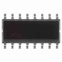
IC MULTIVIBRATR MONO DUAL 16SOIC

HCF4538M013TR

Manufacturer Part Number
HCF4538M013TR
Description
IC MULTIVIBRATR MONO DUAL 16SOIC
Manufacturer
STMicroelectronics
Series
4000r
Datasheet

Specifications of HCF4538M013TR

Logic Type
Monostable
Independent Circuits
2
Schmitt Trigger Input
Yes
Propagation Delay
100ns
Current - Output High, Low
6.8mA, 6.8mA
Voltage - Supply
3 V ~ 20 V
Operating Temperature
-55°C ~ 125°C
Mounting Type
Surface Mount
Package / Case
16-SOIC (3.9mm Width)
Elements Per Chip
2
Logic Family
4000B
Propagation Delay Time
600 ns, 300 ns, 200 ns
High Level Output Current
- 2.8 mA
Low Level Output Current
2.8 mA
Supply Voltage (max)
20 V
Supply Voltage (min)
3 V
Maximum Power Dissipation
100 mW
Maximum Operating Temperature
+ 125 C
Minimum Operating Temperature
- 55 C
Mounting Style
SMD/SMT
Operating Supply Voltage
3.3 V, 5 V, 9 V, 12 V
Lead Free Status / RoHS Status
Lead free / RoHS Compliant
Other names
497-1146-2

Available stocks

Company
Part Number
Manufacturer
Quantity
Price
Part Number:
HCF4538M013TR
Manufacturer:
SOLOMON
Quantity:
4 900
Part Number:
HCF4538M013TR
Manufacturer:
ST
0
DESCRIPTION
The HCF4538B is a monolithic integrated circuit
fabricated
technology available in DIP and SOP packages.
The
multivibrator
resettable one-shot operation for any fixed voltage
PIN CONNECTION
September 2001
RETRIGGERABLE/RESETTABLE
CAPABILITY
TRIGGER AND RESET PROPAGATION
DELAYS INDEPENDENT OF R
TRIGGERING FROM LEADING OR
TRAILING EDGE
Q AND Q BUFFERED OUTPUT AVAILABLE
SEPARATE RESETS
WIDE RANGE OF OUTPUT PULSE WIDTHS
QUIESCENT CURRENT SPECIFIED UP TO
20V
5V, 10V AND 15V PARAMETRIC RATINGS
SCHMITT TRIGGER INPUT ALLOWS
UNLIMITED RISE AND FALL TIMES ON +TR
AND -TR INPUTS
INPUT LEAKAGE CURRENT
I
100% TESTED FOR QUIESCENT CURRENT
MEETS ALL REQUIREMENTS OF JEDEC
JESD13B " STANDARD SPECIFICATIONS
FOR DESCRIPTION OF B SERIES CMOS
DEVICES"
I
= 100nA (MAX) AT V
HCF4538B
in
provides
Metal
dual
Oxide
DD
precision
stable
= 18V T
Semiconductor
X
, C
retriggerable/
DUAL MONOSTABLE MULTIVIBRATOR
A
monostable
X
= 25°C
ORDER CODES
timing application. An external resistor (R
an external capacitor (C
accuracy for the circuit. Adjustment of R
provides a wide range of output pulse widths from
the Q and Q terminals. The time delay from trigger
input to output transition (trigger propagation
delay) and the time delay from reset input to
output transition (reset propagation delay) and the
time delay from reset input to output transition
(reset propagation delay) are independent of R
and C
achieved through linear CMOS techniques.
Leading edge triggering (+TR) and trailing edge
triggering (-TR) inputs are provided for triggering
PACKAGE
SOP
DIP
X
. Precision control of output pulse width is
DIP
HCF4538BM1
HCF4538BEY
TUBE
X
) control the timing and
HCF4538B
HCF4538M013TR
SOP
T & R
X
and C
X
) and
1/10
X
X

Related parts for HCF4538M013TR

HCF4538M013TR Summary of contents

Page 1

... C . Precision control of output pulse width is X achieved through linear CMOS techniques. monostable Leading edge triggering (+TR) and trailing edge retriggerable/ triggering (-TR) inputs are provided for triggering HCF4538B DIP SOP TUBE T & R HCF4538BEY HCF4538BM1 HCF4538M013TR ) control the timing and X and and 1/10 ...

Page 2

HCF4538B from either edge of an input pulse. An unused +TR input should be tied unused -TR input SS should be tied RESET (on low level provided for immediate termination ...

Page 3

TABLE 1 : Functional Terminal Connections V DD FUNCTION Mono (1) Mono (2) Mono (1) Mono (2) Mono (1) Mono (2) Mono (1) Mono (2) Leading Edge Trigger Retriggerable Leading Edge Trigger/Non 3 Retriggerable Trailing Edge Trigger/ 3 ...

Page 4

HCF4538B LOGIC DIAGRAM ABSOLUTE MAXIMUM RATINGS Symbol V Supply Voltage Input Voltage Input Current I P Power Dissipation per Package D Power Dissipation per Output Transistor T Operating Temperature op T Storage Temperature stg ...

Page 5

DC SPECIFICATIONS Symbol Parameter V (V) I Quiescent Current 0/5 L 0/10 0/15 0/20 V High Level Output 0/5 OH Voltage 0/10 0/15 V Low Level Output 5/0 OL Voltage 10/0 15/0 V High Level Input IH Voltage V Low ...

Page 6

HCF4538B DYNAMIC ELECTRICAL CHARACTERISTICS (T Symbol Parameter t t Transition Time TLH THL t t Propagation Delay Time PLH PHL + Propagation Delay Time PLH PHL Reset ...

Page 7

TEST CIRCUIT C = 50pF or equivalent (includes jig and probe capacitance 200K pulse generator (typically OUT WAVEFORM : PROPAGATION DELAY TIMES (f=1MHz; 50% duty cycle) HCF4538B 7/10 ...

Page 8

HCF4538B DIM. MIN. a1 0. 8/10 Plastic DIP-16 (0.25) MECHANICAL DATA mm. TYP MAX. 1.65 0.5 0.25 20 8.5 2.54 17.78 7.1 5.1 3.3 1.27 inch MIN. TYP. ...

Page 9

SO-16 MECHANICAL DATA mm. DIM. MIN 0 0. 9 3.8 G 4 TYP MAX. MIN. 1.75 0.2 0.003 1.65 0.46 0.013 0.25 ...

Page 10

... No license is granted by implication or otherwise under any patent or patent rights of STMicroelectronics. Specifications mentioned in this publication are subject to change without notice. This publication supersedes and replaces all information previously supplied ...

Related keywords