HCF4098BEY STMicroelectronics, HCF4098BEY Datasheet
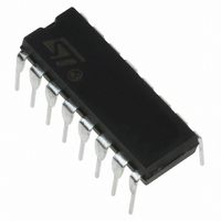
IC MULTIVIBRATOR DUAL 16-DIP

HCF4098BEY

Manufacturer Part Number
HCF4098BEY
Description
IC MULTIVIBRATOR DUAL 16-DIP
Manufacturer
STMicroelectronics
Series
4000Br
Datasheets

Specifications of HCF4098BEY

Logic Type
Monostable
Independent Circuits
2
Schmitt Trigger Input
No
Propagation Delay
100ns
Current - Output High, Low
6.8mA, 6.8mA
Voltage - Supply
3 V ~ 20 V
Operating Temperature
-55°C ~ 125°C
Mounting Type
Through Hole
Package / Case
16-DIP (0.300", 7.62mm)
Elements Per Chip
2
Logic Family
4000B
Input Bias Current (max)
0.02 mA
Propagation Delay Time
500 ns, 250 ns, 200 ns
High Level Output Current
- 2.8 mA
Low Level Output Current
2.8 mA
Supply Voltage (max)
20 V
Supply Voltage (min)
3 V
Maximum Operating Temperature
+ 125 C
Minimum Operating Temperature
- 55 C
Mounting Style
Through Hole
Operating Supply Voltage
3.3 V, 5 V, 9 V, 12 V
Circuit Type
Monolithic Integrated
Current, Supply
600 μA
Logic Function
Multivibrator
Number Of Circuits
Dual
Package Type
DIP-16
Special Features
Retriggerable/Resettable Monostable
Temperature, Operating, Range
-55 to +125 °C
Voltage, Supply
3 to 20 V
Lead Free Status / RoHS Status
Lead free / RoHS Compliant

Available stocks

Company
Part Number
Manufacturer
Quantity
Price
Part Number:
HCF4098BEY
Manufacturer:
IDT
Quantity:
1 832
Part Number:
HCF4098BEY
Manufacturer:
ST
0
Company:
Part Number:
HCF4098BEY
Quantity:
5 000
Part Number:
HCF4098BEY (PB)
Manufacturer:
ST
0
DESCRIPTION
The HCF4098B is a monolithic integrated circuit
fabricated
technology available in DIP and SOP packages.
The
multivibrator
resettable one-shot operation for any fixed voltage
timing application. An external resistor (R
an external capacitor (C
the circuit. Adjustment of R
PIN CONNECTION
September 2001
RETRIGGERABLE/RESETTABLE
CAPABILITY
TRIGGER AND RESET PROPAGATION
DELAYS INDEPENDENT OF R
TRIGGERING FROM LEADING OR
TRAILING EDGE
Q AND Q BUFFERED OUTPUT AVAILABLE
SEPARATE RESETS
WIDE RANGE OF OUTPUT PULSE WIDTHS
QUIESCENT CURRENT SPECIFIED UP TO
20V
5V, 10V AND 15V PARAMETRIC RATINGS
INPUT LEAKAGE CURRENT
I
100% TESTED FOR QUIESCENT CURRENT
MEETS ALL REQUIREMENTS OF JEDEC
JESD13B " STANDARD SPECIFICATIONS
FOR DESCRIPTION OF B SERIES CMOS
DEVICES"
I
= 100nA (MAX) AT V
HCF4098B
in
provides
Metal
dual
X
Oxide
DD
) control the timing for
precision
stable
X
= 18V T
and C
Semiconductor
X
, C
retriggerable/
X
DUAL MONOSTABLE MULTIVIBRATOR
A
monostable
X
= 25°C
provides a
X
) and
ORDER CODES
wide range of output pulse widths from the Q and
Q terminals. The time delay from trigger input to
output transition (trigger propagation delay) and
the time delay from reset input to output transition
(reset propagation delay) and the time delay from
reset input to output transition (reset propagation
delay) are independent of R
edge triggering (+TR) and trailing edge triggering
(-TR) inputs are provided for triggering from either
edge of an input pulse. An unused +TR input
should be tied to V
be tied to V
for immediate termination of the output pulse or to
prevent output pulses when power is turned on.
PACKAGE
SOP
DIP
DD
DIP
HCF4098BM1
. A RESET (on low level) is provided
HCF4098BEY
TUBE
SS
. An unused -TR input should
HCF4098B
X
HCF4098M013TR
and C
SOP
T & R
X
. Leading
1/10

Related parts for HCF4098BEY

HCF4098BEY Summary of contents

Page 1

... An unused +TR input retriggerable/ should be tied tied and X for immediate termination of the output pulse or to prevent output pulses when power is turned on. and C provides a X HCF4098B DIP SOP TUBE T & R HCF4098BEY HCF4098BM1 HCF4098M013TR and C . Leading unused -TR input should RESET (on low level) is provided DD 1/10 ...

Page 2

HCF4098B An unused RESET input should be tied to V However entire section of the HCF4098B is not used, its reset should be tied to V 1). In normal operation the circuit triggers (extends the output pulse one ...

Page 3

TABLE 1 : Functional Terminal Connections V DD FUNCTION Mono (1) Mono (2) Mono (1) Mono (2) Mono (1) Mono (2) Mono (1) Mono (2) Leading Edge Trigger Retriggerable Leading Edge Trigger/Non 3 Retriggerable Trailing Edge Trigger/ 3 ...

Page 4

HCF4098B RECOMMENDED OPERATING CONDITIONS Symbol V Supply Voltage DD V Input Voltage I T Operating Temperature op DC SPECIFICATIONS Symbol Parameter V (V) I Quiescent Current 0/5 L 0/10 0/15 0/20 V High Level Output 0/5 OH Voltage 0/10 0/15 ...

Page 5

DYNAMIC ELECTRICAL CHARACTERISTICS (T Symbol Parameter t t Propagation Delay Time PLH PHL + Trigger Pulse Width Transition Time TLH t Transition Time THL t t Propagation Delay Time ...

Page 6

HCF4098B TEST CIRCUIT C = 50pF or equivalent (includes jig and probe capacitance 200K pulse generator (typically OUT 6/10 ...

Page 7

HCF4098B 7/10 ...

Page 8

HCF4098B DIM. MIN. a1 0. 8/10 Plastic DIP-16 (0.25) MECHANICAL DATA mm. TYP MAX. 1.65 0.5 0.25 20 8.5 2.54 17.78 7.1 5.1 3.3 1.27 inch MIN. TYP. ...

Page 9

SO-16 MECHANICAL DATA mm. DIM. MIN 0 0. 9 3.8 G 4 TYP MAX. MIN. 1.75 0.2 0.003 1.65 0.46 0.013 0.25 ...

Page 10

... No license is granted by implication or otherwise under any patent or patent rights of STMicroelectronics. Specifications mentioned in this publication are subject to change without notice. This publication supersedes and replaces all information previously supplied ...

Related keywords