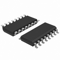
74HC166D,652 NXP Semiconductors, 74HC166D,652 Datasheet - Page 15

74HC166D,652
Manufacturer Part Number
74HC166D,652
Description
IC 8BIT SHIFT REGISTER 16-SOIC
Manufacturer
NXP Semiconductors
Series
74HCr
Datasheets
1.74HCT4046ADB112.pdf
(19 pages)
2.74HCT4046ADB112.pdf
(23 pages)
3.74HC166N652.pdf
(10 pages)
Specifications of 74HC166D,652
Logic Type
Shift Register
Output Type
Standard
Number Of Elements
1
Number Of Bits Per Element
8
Function
Parallel or Serial to Serial
Voltage - Supply
2 V ~ 6 V
Operating Temperature
-40°C ~ 125°C
Mounting Type
Surface Mount
Package / Case
16-SOIC (3.9mm Width)
Lead Free Status / RoHS Status
Lead free / RoHS Compliant
Other names
568-2624-5
933714550652
933714550652
Philips Semiconductors
DATA SHEET SPECIFICATION GUIDE
INTRODUCTION
The 74HCMOS data sheets have been designed for
ease-of-use. A minimum of cross-referencing for more
information is needed.
TYPICAL PROPAGATION DELAY AND FREQUENCY
The typical propagation delays listed at the top of the data
sheets are the average of t
path through the device with a 15 pF load.
For clocked devices, the maximum frequency of operation
is also given. The typical operating frequency is the
maximum device operating frequency with a 50% duty
factor and no constraints on t
LOGIC SYMBOLS
Two logic symbols are given for each device - the
conventional one (Logic Symbol) which explicitly shows
the internal logic (except for complex logic) and the IEC
Logic Symbol as developed by the IEC (International
Electrotechnical Commission).
The IEC has been developing a very powerful symbolic
language that can show the relationship of each input of a
digital logic current to each output without explicitly
showing the internal logic.
Internationally, Working Group 2 of IEC Technical
Committee TC-3 has prepared a new document
(Publication 617-12) which supersedes
Publication 117-15, published in 1972.
RATINGS
The “RATINGS” table (Limiting values in accordance with
the Absolute Maximum System - IEC134) lists the
maximum limits to which the device can be subjected
without damage. This doesn’t imply that the device will
function at these extreme conditions, only that, when these
conditions are removed and the device operated within the
Recommended Operating Conditions, it will still be
functional and its useful life won’t have been shortened.
The maximum rated supply voltage of 7 V is well below the
typical breakdown voltage of 18 V.
RECOMMENDED OPERATING CONDITIONS
The “RECOMMENDED OPERATING CONDITIONS”
table lists the operating ambient temperature and the
March 1988
HCMOS family characteristics
PLH
r
and t
and t
PHL
f
.
for the longest data
15
conditions under which the limits in the “DC
CHARACTERISTICS” and “AC CHARACTERISTICS”
tables will be met. The table should not be seen as a set of
limits guaranteed by the manufacturer, but as the
conditions used to test the devices and guarantee that
they will then meet the limits in the DC and AC
CHARACTERISTICS tables.
DC CHARACTERISTICS
The “DC CHARACTERISTICS” table reflects the DC limits
used during testing. The values published are guaranteed.
The threshold values of V
user. If V
voltages will be those published in the “DC
CHARACTERISTICS” table. There is a tendency, by
some, to use the published V
device for functionality in a “function-table exercizer”
mode. This frequently causes problems because of the
noise present at the test head of automated test
equipment with cables up to 1 metre. Parametric tests,
such as those used for the output levels under the V
V
milliseconds, so that there is no noise at the inputs when
the outputs are measured. But in functionality testing, the
outputs are measured much faster, so there can be noise
on the inputs, before the device has assumed its final and
correct output state. Thus, never use V
functionality of any HCMOS device type; instead, use input
voltages of V
state). In no way does this imply that the devices are
noise-sensitive in the final system.
In the data sheets, it may appear strange that the typical
V
because V
devices that will be recognized as a logic LOW. However,
typically a higher V
LOW. Conversely, the typical V
guaranteed level.
For 74HCMOS, unlike TTL, no output HIGH short-circuit
current is specified. The use of this current, for example, to
calculate propagation delays with capacitive loads, is
covered by the HCMOS graphs showing the output drive
capability and those showing the dependence of
propagation delay on load capacitance.
The quiescent supply current I
all the reversed-biased diodes and the OFF-state MOS
transistors. It is measured with the inputs at V
and is typically a few nA.
IL
IL
conditions are done fairly slowly, in the order of
is higher than the maximum V
IH
ILmax
and V
CC
FAMILY SPECIFICATIONS
(for the HIGH state) and 0 V (for the LOW
is the maximum V
IL
are applied to the inputs, the output
IL
will also be recognized as a logic
IH
and V
IH
CC
IH
and V
is lower than its minimum
is the leakage current of
IL
IL
IL
. However, this is
can be tested by the
(guaranteed) for all
IL
IH
thresholds to test a
and V
CC
IL
to test the
or GND
IH
and


