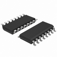
74HC166D,652 NXP Semiconductors, 74HC166D,652 Datasheet - Page 18

74HC166D,652
Manufacturer Part Number
74HC166D,652
Description
IC 8BIT SHIFT REGISTER 16-SOIC
Manufacturer
NXP Semiconductors
Series
74HCr
Datasheets
1.74HCT4046ADB112.pdf
(19 pages)
2.74HCT4046ADB112.pdf
(23 pages)
3.74HC166N652.pdf
(10 pages)
Specifications of 74HC166D,652
Logic Type
Shift Register
Output Type
Standard
Number Of Elements
1
Number Of Bits Per Element
8
Function
Parallel or Serial to Serial
Voltage - Supply
2 V ~ 6 V
Operating Temperature
-40°C ~ 125°C
Mounting Type
Surface Mount
Package / Case
16-SOIC (3.9mm Width)
Lead Free Status / RoHS Status
Lead free / RoHS Compliant
Other names
568-2624-5
933714550652
933714550652
Philips Semiconductors
AC switching parameters
March 1988
f
f
f
t
t
t
t
t
t
i
o
max
h
r
f
PHL
PLH
PHZ
,
HCMOS family characteristics
Input frequency; for combinatorial logic devices
the maximum number of inputs and outputs
switching in accordance with the device
function table. For sequential logic devices the
clock frequency using alternate HIGH and LOW
for data input or using the toggle mode,
whichever is applicable.
Output frequency; each output.
Maximum clock frequency; clock input
waveforms should have a 50% duty factor and
be such as to cause the outputs to be switching
from 10%V
the device function table.
Hold time; the interval immediately following the
active transition of the timing pulse (usually the
clock pulse) or following the transition of the
control input to its latching level, during which
interval the data to be recognized must be
maintained at the input to ensure their
continued recognition. A negative hold time
indicates that the correct logic level may be
released prior to the timing pulse and still be
recognized.
Clock input rise and fall times; 10% and 90%
values.
Propagation delay; the time between the
specified reference points, normally the 50%
points for 74HC and 74HCU devices on the
input and output waveforms and the 1.3 V
points for the 74HCT devices, with the output
changing from the defined HIGH level to the
defined LOW level.
Propagation delay; the time between the
specified reference points, normally the 50%
points for 74HC and 74HCU devices on the
input and output waveforms and the 1.3 V point
for the 74HCT devices, with the output
changing from the defined LOW level to the
defined HIGH level.
3-state output disable time; the time between
the specified reference points, normally the
50% points for the 74HC and 74HCU devices
and the 1.3 V points for the 74HCT devices on
the output enable input voltage waveform and a
point representing 10% of the output swing on
the output voltage waveform of a 3-state
device, with the output changing from
a HIGH level (V
OFF-state (Z).
CC
to 90%V
OH
) to a high impedance
CC
in accordance with
18
t
t
t
t
t
PLZ
PZH
PZL
rem
su
3-state output disable time; the time between
the specified reference points, normally the
50% points for the 74HC devices and the 1.3 V
points for the 74HCT devices on the output
enable input voltage waveform and a point
representing 10% of the output swing on the
output voltage waveform of a 3-state
device, with the output changing from a LOW
level (V
3-state output enable time; the time between
the specified reference points, normally the
50% points for the 74HC devices and 1.3 V
points for the 74HCT devices on the output
enable input voltage waveform and the 50%
point on the output voltage waveform of a
3-state device, with the output changing from a
high impedance OFF-state (Z) to a HIGH level
(V
3-state output enable time; the time between
the specified reference points, normally the
50% points for the 74HC devices and the 1.3 V
points for the 74HCT devices on the output
enable input voltage waveform and the 50%
point on the output voltage waveform of a
3-state device, with the output changing from a
high impedance OFF-state (Z) to a LOW level
(V
Removal time; the time between the end of an
overriding asynchronous input, typically a clear
or reset input, and the earliest permissible
beginning of a synchronous control input,
typically a clock input, normally measured at
the 50% points for 74HC devices and the 1.3 V
points for the 74HCT devices on both input
voltage waveforms.
Set-up time; the interval immediately preceding
the active transition of the timing pulse (usually
the clock pulse) or preceding the transition of
the control input to its latching level, during
which interval the data to be recognized must
be maintained at the input to ensure their
recognition. A negative set-up time indicates
that the correct logic level may be initiated
sometime after the active transition of the
timing pulse and still be recognized.
OH
OL
).
).
FAMILY SPECIFICATIONS
OL
) to a high impedance OFF-state (Z).


