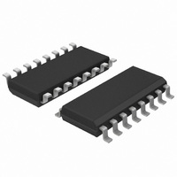
74HC165D,652 NXP Semiconductors, 74HC165D,652 Datasheet - Page 11

74HC165D,652
Manufacturer Part Number
74HC165D,652
Description
IC SHIFT REGST 8BIT PI-SO 16SOIC
Manufacturer
NXP Semiconductors
Series
74HCr
Type
Not Requiredr
Datasheet
1.74HCT165N652.pdf
(22 pages)
Specifications of 74HC165D,652
Package / Case
16-SOIC (3.9mm Width)
Logic Type
Shift Register
Output Type
Differential
Function
Parallel or Serial to Serial
Number Of Elements
1
Number Of Bits Per Element
8
Voltage - Supply
2 V ~ 6 V
Operating Temperature
-40°C ~ 125°C
Mounting Type
Surface Mount
Counting Sequence
Serial/Parallel to Serial
Number Of Circuits
1
Logic Family
HC
Propagation Delay Time
165 ns, 33 ns, 28 ns
Supply Voltage (max)
7 V
Maximum Operating Temperature
+ 125 C
Minimum Operating Temperature
- 40 C
Mounting Style
SMD/SMT
Operating Supply Voltage
2 V to 6 V
Supply Voltage (min)
0.5 V
Technology
CMOS
Number Of Elements
1
Number Of Bits
8
Logical Function
Shift Register
Operating Supply Voltage (typ)
5V
Package Type
SO
Operating Temp Range
-40C to 125C
Operating Supply Voltage (min)
2V
Operating Supply Voltage (max)
6V
Operating Temperature Classification
Automotive
Mounting
Surface Mount
Pin Count
16
Lead Free Status / RoHS Status
Lead free / RoHS Compliant
Lead Free Status / RoHS Status
Lead free / RoHS Compliant, Lead free / RoHS Compliant
Other names
568-3954-5
74HC165D
74HC165D
933713780652
74HC165D
74HC165D
933713780652
NXP Semiconductors
Table 7.
GND (ground = 0 V); C
[1]
[2]
[3]
12. Waveforms
74HC_HCT165_3
Product data sheet
Symbol Parameter
C
Fig 7.
PD
t
t
C
P
f
f
C
V
pd
t
i
o
D
CC
is the same as t
PD
= input frequency in MHz;
L
(C
= output frequency in MHz;
is the same as t
= output load capacitance in pF;
= C
L
= supply voltage in V.
is used to determine the dynamic power dissipation (P
power
dissipation
capacitance
Measurement points are given in
V
The clock (CP) or clock enable (CE) to output (Q7 or Q7) propagation delays, the clock pulse width, the
maximum clock frequency and the output transition times
PD
V
OL
Dynamic characteristics
CC
and V
V
2
CC
f
2
o
) = sum of outputs;
OH
THL
PHL
f
i
are typical voltage output levels that occur with the output load.
L
+
and t
= 50 pF unless otherwise specified; for test circuit, see
and t
Conditions
per package;
V
(C
I
Q7 or Q7 output
TLH
CP or CE input
= GND to V
L
PLH
.
V
.
CC
2
f
…continued
o
) where:
CC
Table
GND
V
V
OH
OL
V
I
1.5 V
8.
Rev. 03 — 14 March 2008
V
M
t
PHL
[3]
D
t
in W).
W
Min
-
1/f
V
M
max
25 C
t
Typ Max
THL
35
-
74HC165; 74HCT165
8-bit parallel-in/serial out shift register
Figure 12
40 C to +85 C
t
Min
t
TLH
PLH
-
Max
mna987
-
40 C to +125 C Unit
Min
-
© NXP B.V. 2008. All rights reserved.
Max
-
11 of 22
pF


