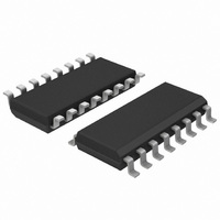
74HC165D,652 NXP Semiconductors, 74HC165D,652 Datasheet - Page 13

74HC165D,652
Manufacturer Part Number
74HC165D,652
Description
IC SHIFT REGST 8BIT PI-SO 16SOIC
Manufacturer
NXP Semiconductors
Series
74HCr
Type
Not Requiredr
Datasheet
1.74HCT165N652.pdf
(22 pages)
Specifications of 74HC165D,652
Package / Case
16-SOIC (3.9mm Width)
Logic Type
Shift Register
Output Type
Differential
Function
Parallel or Serial to Serial
Number Of Elements
1
Number Of Bits Per Element
8
Voltage - Supply
2 V ~ 6 V
Operating Temperature
-40°C ~ 125°C
Mounting Type
Surface Mount
Counting Sequence
Serial/Parallel to Serial
Number Of Circuits
1
Logic Family
HC
Propagation Delay Time
165 ns, 33 ns, 28 ns
Supply Voltage (max)
7 V
Maximum Operating Temperature
+ 125 C
Minimum Operating Temperature
- 40 C
Mounting Style
SMD/SMT
Operating Supply Voltage
2 V to 6 V
Supply Voltage (min)
0.5 V
Technology
CMOS
Number Of Elements
1
Number Of Bits
8
Logical Function
Shift Register
Operating Supply Voltage (typ)
5V
Package Type
SO
Operating Temp Range
-40C to 125C
Operating Supply Voltage (min)
2V
Operating Supply Voltage (max)
6V
Operating Temperature Classification
Automotive
Mounting
Surface Mount
Pin Count
16
Lead Free Status / RoHS Status
Lead free / RoHS Compliant
Lead Free Status / RoHS Status
Lead free / RoHS Compliant, Lead free / RoHS Compliant
Other names
568-3954-5
74HC165D
74HC165D
933713780652
74HC165D
74HC165D
933713780652
NXP Semiconductors
Table 8.
74HC_HCT165_3
Product data sheet
Type
74HC165
74HCT165
Fig 10. The set-up and hold times from the serial data input (DS) to the clock (CP) and clock enable (CE) inputs,
Fig 11. The set-up and hold times from the data inputs (Dn) to the parallel load input (PL)
(1) CE may change only from HIGH-to-LOW while CP is LOW, see
The shaded areas indicate when the input is permitted to change for predictable output performance
Measurement points are given in
V
from the clock enable input (CE) to the clock input (CP) and from the clock input (CP) to the
clock enable input (CE)
Measurement points are given in
V
OL
OL
Measurement points
and V
and V
OH
OH
are typical voltage output levels that occur with the output load.
are typical voltage output levels that occur with the output load.
Dn input
PL input
CP, CE input
CP, CE input
GND
GND
DS input
V
V
Input
V
V
3 V
I
I
I
CC
GND
GND
GND
V
V
V
Table
Table
V
I
I
I
M
t
su
8.
8.
(1)
V
Rev. 03 — 14 March 2008
M
V
V
t
su
M
M
t
t
h
su
V
t
h
M
V
0.5V
1.3 V
M
Section
CC
1.
V
74HC165; 74HCT165
M
t
W
8-bit parallel-in/serial out shift register
t
su
t
su
V
M
t
t
h
h
mna990
mna991
Output
V
0.5V
1.3 V
M
CC
© NXP B.V. 2008. All rights reserved.
13 of 22


