MC14549BCPG ON Semiconductor, MC14549BCPG Datasheet
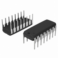
IC REGISTER 8BIT APPROX 16-DIP

MC14549BCPG

Manufacturer Part Number
MC14549BCPG
Description
IC REGISTER 8BIT APPROX 16-DIP
Manufacturer
ON Semiconductor
Series
4000Br
Datasheet

Specifications of MC14549BCPG

Logic Type
Register, Successive Approximation
Output Type
Standard
Number Of Elements
1
Number Of Bits Per Element
8
Function
Universal
Voltage - Supply
3 V ~ 18 V
Operating Temperature
-55°C ~ 125°C
Mounting Type
Through Hole
Package / Case
16-DIP (0.300", 7.62mm)
Lead Free Status / RoHS Status
Lead free / RoHS Compliant
MC14549B, MC14559B
Successive Approximation
Registers
registers are 8−bit registers providing all the digital control and storage
necessary for successive approximation analog−to−digital conversion
systems. These parts differ in only one control input. The Master Reset
(MR) on the MC14549B is required in the cascaded mode when more
than 8 bits are desired. The Feed Forward (FF) of the MC14559B is
used for register shortening where End−of−Conversion (EOC) is
required after less than eight cycles.
analog−to−digital conversion, with serial and parallel outputs.
Features
Stresses exceeding Maximum Ratings may damage the device. Maximum
Ratings are stress ratings only. Functional operation above the Recommended
Operating Conditions is not implied. Extended exposure to stresses above the
Recommended Operating Conditions may affect device reliability.
1. Temperature Derating:
static voltages or electric fields. However, precautions must be taken to avoid
applications of any voltage higher than maximum rated voltages to this
high−impedance circuit. For proper operation, V
the range V
(e.g., either V
*For additional information on our Pb−Free strategy and soldering details, please
MAXIMUM RATINGS
© Semiconductor Components Industries, LLC, 2006
June, 2006 − Rev. 6
download the ON Semiconductor Soldering and Mounting Techniques
Reference Manual, SOLDERRM/D.
DC Supply Voltage Range
Input Voltage Range, All Inputs
DC Input Current per Pin
Power Dissipation per Package (Note 1)
Operating Temperature Range
Storage Temperature Range
The MC14549B and MC14559B successive approximation
Applications for the MC14549B and MC14559B include
This device contains protection circuitry to guard against damage due to high
Unused inputs must always be tied to an appropriate logic voltage level
MC1408 8−Bit D/A Converter
TTL Load or 2 HTL Loads Over the Rated Temperature Range
Totally Synchronous Operation
All Outputs Buffered
Single Supply Operation
Serial Output
Retriggerable
Compatible with a Variety of Digital and Analog Systems such as the
All Control Inputs Positive−Edge Triggered
Supply Voltage Range = 3.0 Vdc to 18 Vdc
Capable of Driving 2 Low−Power TTL Loads, 1 Low−Power Schottky
Chip Complexity: 488 FETs or 122 Equivalent Gates
Pb−Free Packages are Available*
Plastic “P and D/DW” Packages: – 7.0 mW/_C From 65_C To 125_C
SS
SS
v (V
Parameter
or V
in
DD
or V
).
(Voltages Referenced to V
out
) v V
DD
.
Symbol
V
T
V
P
in
T
I
DD
stg
in
in
D
A
and V
SS
out
−0.5 to V
)
−0.5 to +18.0
−55 to +125
−65 to +150
should be constrained to
Value
±10
500
DD
+ 0.5
1
Unit
mW
mA
°C
°C
V
V
See detailed ordering and shipping information in the package
dimensions section on page 3 of this data sheet.
1
1
*For MC14549B Pin 10 is MR input.
For MC14559B Pin 10 is FF input.
ORDERING INFORMATION
x
A
WL = Wafer Lot
YY
WW = Work Week
G
S
V
Q4
Q5
Q6
Q7
http://onsemi.com
out
PIN ASSIGNMENT
SS
DW SUFFIX
CASE 751G
D
C
SO−16W
= 4 or 5
= Assembly Location
= Year
= Pb−Free Package
CASE 648
P SUFFIX
PDIP−16
1
2
3
4
5
6
7
8
Publication Order Number:
16
15
14
13
12
10
11
16
9
16
1
1
Q3
V
Q2
Q1
Q0
EOC
*
SC
DIAGRAMS
MC145x9BCP
AWLYYWWG
DD
MARKING
AWLYYWWG
MC145x9B
MC14549B/D

Related parts for MC14549BCPG

MC14549BCPG Summary of contents

Page 1

... Unused inputs must always be tied to an appropriate logic voltage level (e.g., either *For additional information on our Pb−Free strategy and soldering details, please download the ON Semiconductor Soldering and Mounting Techniques Reference Manual, SOLDERRM/D. © Semiconductor Components Industries, LLC, 2006 June, 2006 − Rev Symbol ...

Page 2

MC14549B SC SC MR( ) Clock t−1 t− Don’t Care t−1 = ...

Page 3

... Pulse Width — Clock Rise and Fall Time Clock Pulse Frequency 5. The formulas given are for the typical characteristics only. ORDERING INFORMATION Device MC14549BCP MC14549BCPG MC14549BDWR2 MC14549BDWR2G MC14559BCP MC14559BCPG MC14559BDWR2 MC14559BDWR2G †For information on tape and reel specifications, including part orientation and tape sizes, please refer to our Tape and Reel Packaging Specifications Brochure, BRD8011/D ...

Page 4

SWITCHING TIME TEST CIRCUIT AND WAVEFORMS PROGRAMMABLE Q3 PULSE Q2 GENERATOR FF(MR EOC S out V SS CLOCK SC D É É Q7 É É É É ...

Page 5

Both the MC14549B and MC14559B can be operated in either the “free run” or “strobed operation” mode for conversion schemes with any number of bits. Reliable cascading and/or recirculating operation can be achieved if the End of Convert (EOC) output ...

Page 6

Externally Controlled 6−Bit ADC (Figure 2) Several features are shown in this application: • Shortening of the register to six bits by feeding the seventh output bit into the FF input. • Continuous conversion continuous signal is applied ...

Page 7

C SC MC14559B DAC Externally Controlled 12−Bit ADC (Figure 5) In this circuit the external pulse starts the first SAR and simultaneously resets the cascaded second SAR. When Q4 of the ...

Page 8

−T− 0.25 (0.010 16X 0. SEATING e PLANE 14X ...

Page 9

... Opportunity/Affirmative Action Employer. This literature is subject to all applicable copyright laws and is not for resale in any manner. PUBLICATION ORDERING INFORMATION LITERATURE FULFILLMENT: Literature Distribution Center for ON Semiconductor P.O. Box 5163, Denver, Colorado 80217 USA Phone: 303−675−2175 or 800−344−3860 Toll Free USA/Canada Fax: 303− ...

Related keywords