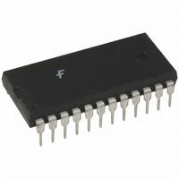
MM74C905N Fairchild Semiconductor, MM74C905N Datasheet

MM74C905N
Specifications of MM74C905N
74C905N
Available stocks
Related parts for MM74C905N
MM74C905N Summary of contents
Page 1
... Ordering Code: Order Number Package Number MM74C905N N24A 24-Lead Plastic Dual-In-Line Package (PDIP), JEDEC MS-011, 0.600" Wide Connection Diagram © 2003 Fairchild Semiconductor Corporation Features Wide supply voltage range: Guaranteed noise margin: 1 ...
Page 2
Truth Table Time Inputs Q11 D11 D10 H L D11 D11 D10 D11 ...
Page 3
Absolute Maximum Ratings Voltage at Any Pin 0. Operating Temperature Range ( Storage Temperature Range ( Power Dissipation ( Dual-In-Line Small Outline Operating V Range CC Absolute ...
Page 4
AC Electrical Characteristics pF, unless otherwise specified A L Symbol Parameter t Propagation Delay Time from pd Clock Input to Outputs (Q0–Q11 pd(Q) t Propagation Delay Time from pd Clock Input to D0 ...
Page 5
Timing Diagram 5 www.fairchildsemi.com ...
Page 6
Switching Time Waveforms USER NOTES FOR A/D CONVERSION The register can be used with either current switches that require a low voltage level to turn the switch ON or current switches that require a high voltage level to turn the ...
Page 7
Typical Applications 12-Bit Successive Approximation A-to-D Converter, Operating in Continuous 8–Bit Truncated Mode 12-Bit Successive Approximation A-to-D Converter, Operating in Continuous Mode, Drives the 50k/100k Ladder Network Directly Definition of Terms CP: Register clock input. CC: Conversion complete—this output remains ...
Page 8
Physical Dimensions inches (millimeters) unless otherwise noted 24-Lead Plastic Dual-In-Line Package (PDIP), JEDEC MS-011, 0.600" Wide Fairchild does not assume any responsibility for use of any circuitry described, no circuit patent licenses are implied and Fairchild reserves the right at ...


