CD4016BCM Fairchild Semiconductor, CD4016BCM Datasheet

IC SWITCH BILATERAL QUAD 14-SOIC

CD4016BCM

Manufacturer Part Number
CD4016BCM
Description
IC SWITCH BILATERAL QUAD 14-SOIC
Manufacturer
Fairchild Semiconductor
Series
4000Br
Type
Bilateral, FET Switchesr
Datasheet

Specifications of CD4016BCM

Circuit
1 x 1:1
Independent Circuits
4
Voltage Supply Source
Dual Supply
Voltage - Supply
3 V ~ 15 V
Operating Temperature
-55°C ~ 125°C
Mounting Type
Surface Mount
Package / Case
14-SOIC (3.9mm Width), 14-SOL
Switch Configuration
SPST
On Resistance (max)
2000 Ohms
On Time (max)
50 ns
Off Time (max)
40 ns
Supply Voltage (max)
15 V
Supply Voltage (min)
3 V
Maximum Power Dissipation
500 mW
Maximum Operating Temperature
+ 125 C
Mounting Style
SMD/SMT
Minimum Operating Temperature
- 55 C
Propagation Delay Time
100 ns
Analog Switch Type
SPST
No. Of Channels
4
Bandwidth
40MHz
On State Resistance Max
850ohm
Turn Off Time
10ns
Turn On Time
17ns
Supply Voltage Range
3V To 15V
Rohs Compliant
Yes
Lead Free Status / RoHS Status
Contains lead / RoHS non-compliant
Current - Output High, Low
-
Lead Free Status / Rohs Status
Lead free / RoHS Compliant

Available stocks

Company
Part Number
Manufacturer
Quantity
Price
Part Number:
CD4016BCM
Manufacturer:
SAMSUNG
Quantity:
5
Part Number:
CD4016BCM
Manufacturer:
ST
0
Part Number:
CD4016BCMX
Manufacturer:
FAIRCHILD/仙童
Quantity:
20 000
© 2002 Fairchild Semiconductor Corporation
CD4016BCM
CD4016BCN
CD4016BC
Quad Bilateral Switch
General Description
The CD4016BC is a quad bilateral switch intended for the
transmission or multiplexing of analog or digital signals. It is
pin-for-pin compatible with CD4066BC.
Features
Ordering Code:
Devices also available in Tape and Reel. Specify by appending the letter suffix “X” to the ordering code.
Connection Diagram
Order Number
Wide supply voltage range: 3V to 15V
Wide range of digital and analog switching: 7.5 V
“ON” Resistance for 15V operation: 400 (typ)
Matched “ON” Resistance over 15V signal input:
High degree of linearity:
Extremely low “OFF” switch leakage:
R
0.4% distortion (typ)
@ f
V
0.1 nA (typ.)
@ V
T
ON
DD
A
IS
DD
25 C
V
10 (typ)
SS
1 kHz, V
V
SS
10V, R
Package Number
10V
IS
L
5 V
M14A
N14A
10 k
p-p
,
14-Lead Small Outline Integrated Circuit (SOIC), JEDEC MS-012, 0.150" Narrow
14-Lead Plastic Dual-In-Line Package (PDIP), JEDEC MS-001, 0.300" Wide
DS005661
PEAK
Applications
• Analog signal switching/multiplexing
• Digital signal switching/multiplexing
• CMOS logic implementation
• Analog-to-digital/digital-to-analog conversion
• Digital control of frequency, impedance, phase, and
Schematic Diagram
Extremely high control input impedance: 10
Low crosstalk between switches:
Frequency response, switch “ON”: 40 MHz (typ)
analog-signal gain
@ f
Signal gating
Squelch control
Chopper
Modulator/Demodulator
Commutating switch
50 dB (typ.)
Package Description
IS
0.9 MHz, R
L
1 k
November 1983
Revised March 2002
www.fairchildsemi.com
12
(typ)

Related parts for CD4016BCM

CD4016BCM Summary of contents

Page 1

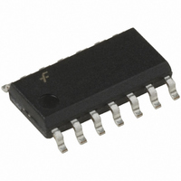
... Ordering Code: Order Number Package Number CD4016BCM M14A 14-Lead Small Outline Integrated Circuit (SOIC), JEDEC MS-012, 0.150" Narrow CD4016BCN N14A 14-Lead Plastic Dual-In-Line Package (PDIP), JEDEC MS-001, 0.300" Wide Devices also available in Tape and Reel. Specify by appending the letter suffix “X” to the ordering code. ...

Page 2

Absolute Maximum Ratings (Note 2) V Supply Voltage DD V Input Voltage 0. Storage Temperature Range S Power Dissipation ( Dual-In-Line Small Outline Lead Temperature (Soldering, 10 seconds) DC Electrical Characteristics Symbol Parameter I ...

Page 3

AC Electrical Characteristics and unless otherwise specified Symbol Parameter Propagation Delay Time PHL PLH Signal Input to Signal Output Propagation Delay ...

Page 4

AC Test Circuits and Switching Time Waveforms FIGURE PLH PLH FIGURE PZH PHZ FIGURE PZH PHZ V V for distortion and frequency response tests ...

Page 5

AC Test Circuits and Switching Time Waveforms FIGURE 5. Crosstalk Between Any Two Switches FIGURE 6. Crosstalk — Control to Input Signal Output FIGURE 7. Maximum Control Input Frequency (Continued) 5 www.fairchildsemi.com ...

Page 6

TABLE 1. CD4016B Switch Test Conditions for V Temperature V V Range COMMERCIAL Typical Performance Characteristics ’ON’ Resistance vs. Signal Voltage ’ON’ ...

Page 7

Typical Applications Special Considerations The CD4016B is composed of 4, two-transistor analog switches. These switches do not have any linearization or compensation circuitry for “R ” the CD4066B's. ON Because of this, the special operating considerations for the ...

Page 8

Physical Dimensions inches (millimeters) unless otherwise noted 14-Lead Small Outline Integrated Circuit (SOIC), JEDEC MS-012, 0.150" Narrow www.fairchildsemi.com Package Number M14A 8 ...

Page 9

Physical Dimensions inches (millimeters) unless otherwise noted (Continued) 14-Lead Plastic Dual-In-Line Package (PDIP), JEDEC MS-001, 0.300" Wide Fairchild does not assume any responsibility for use of any circuitry described, no circuit patent licenses are implied and Fairchild reserves the right ...

Related keywords