74HCT157DB,118 NXP Semiconductors, 74HCT157DB,118 Datasheet
74HCT157DB,118
Specifications of 74HCT157DB,118
74HCT157DB-T
935188560118


Related parts for 74HCT157DB,118


74HCT157DB,118 Summary of contents
Page 1
Quad 2-input multiplexer Rev. 3 — 31 December 2010 1. General description The 74HC157; 74HCT157 is a high-speed Si-gate CMOS device and is pin compatible with Low-power Schottky TTL specified in compliance with JEDEC standard no. ...
Page 2
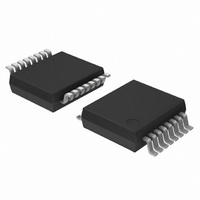
... NXP Semiconductors 3. Ordering information Table 1. Ordering information Type number Package Temperature range 40 C to +125 C 74HC157N 74HCT157N 40 C to +125 C 74HC157D 74HCT157D 40 C to +125 C 74HC157DB 74HCT157DB 40 C to +125 C 74HC157PW 74HCT157PW 40 C to +125 C 74HC157BQ 74HCT157BQ 4 ...
Page 3
... NXP Semiconductors 1I0 2 3 1I1 2I0 5 6 2I1 SELECTOR 11 3I0 3I1 10 14 4I0 13 4I1 S 1 Fig 3. Logic symbol 5. Pinning information 5.1 Pinning 74HC157 74HCT157 S 1 1I0 2 1I1 2I0 5 2I1 GND 8 Fig 5. Pin configuration DIP16, SO16, (T)SSOP16 74HC_HCT157 Product data sheet MULTIPLEXER ...
Page 4
... NXP Semiconductors 5.2 Pin description Table 2. Pin description Symbol Pin Description S 1 common data select input 1I0 to 4I0 2, 5, 11, 14 data inputs from source 0 1I1 to 4I1 3, 6, 10, 13 data inputs from source multiplexer outputs GND 8 ground ( enable input (active LOW supply voltage CC 6 ...
Page 5
... NXP Semiconductors derates linearly with 4.5 mW/K above 60 C. [3] P tot 8. Recommended operating conditions Table 5. Recommended operating conditions Voltages are referenced to GND (ground = 0 V) Symbol Parameter V supply voltage CC V input voltage I V output voltage O T ambient temperature amb t/V input transition rise and fall rate 9 ...
Page 6
... NXP Semiconductors Table 6. Static characteristics At recommended operating conditions; voltages are referenced to GND (ground = 0 V). Symbol Parameter Conditions I supply current 6 input I capacitance 74HCT157 V HIGH-level input voltage V LOW-level input voltage V HIGH-level output voltage = 20 LOW-level output voltage = 20 4.0 mA ...
Page 7
... NXP Semiconductors 10. Dynamic characteristics Table 7. Dynamic characteristics Voltages are referenced to GND (ground = 0 V); C Symbol Parameter Conditions For type 74HC157 t propagation nI0, nI1 to nY; see pd delay nY; see nY; see transition nY; see Figure 7 t time power ...
Page 8
... NXP Semiconductors Table 7. Dynamic characteristics Voltages are referenced to GND (ground = 0 V); C Symbol Parameter Conditions t transition nY; see Figure 7 t time power pF MHz dissipation V = GND capacitance [ the same as t and PLH PHL [ the same as t and THL TLH [ used to determine the dynamic power dissipation (P PD ...
Page 9
... NXP Semiconductors Measurement points are given in V and V are typical voltage output levels that occur with the output load Fig 8. Propagation delay input (E) to output (nY) Table 8. Measurement points Type 74HC157 74HCT157 74HC_HCT157 Product data sheet input M GND t PHL output Table 8. Input ...
Page 10
... NXP Semiconductors Test data is given in Table Definitions test circuit Termination resistance should be equal to output impedance Load capacitance including jig and probe capacitance Load resistance Test selection switch. Fig 9. Test circuit for measuring switching times Table 9. Test data Type Input V I 74HC157 ...
Page 11
... NXP Semiconductors 12. Package outline SO16: plastic small outline package; 16 leads; body width 3 pin 1 index 1 DIMENSIONS (inch dimensions are derived from the original mm dimensions) A UNIT max. 0.25 1.45 mm 1.75 0.25 0.10 1.25 0.010 0.057 inches 0.069 0.01 0.004 0.049 Note 1. Plastic or metal protrusions of 0.15 mm (0.006 inch) maximum per side are not included. ...
Page 12
... NXP Semiconductors SSOP16: plastic shrink small outline package; 16 leads; body width 5 pin 1 index 1 e DIMENSIONS (mm are the original dimensions) A UNIT max. 0.21 1. 0.25 0.05 1.65 Note 1. Plastic or metal protrusions of 0.25 mm maximum per side are not included. OUTLINE VERSION IEC SOT338-1 Fig 11. Package outline SOT338-1 (SSOP16) ...
Page 13
... NXP Semiconductors TSSOP16: plastic thin shrink small outline package; 16 leads; body width 4 pin 1 index 1 DIMENSIONS (mm are the original dimensions) A UNIT max. 0.15 0.95 mm 1.1 0.25 0.05 0.80 Notes 1. Plastic or metal protrusions of 0.15 mm maximum per side are not included. 2. Plastic interlead protrusions of 0.25 mm maximum per side are not included. ...
Page 14
... NXP Semiconductors DHVQFN16: plastic dual in-line compatible thermal enhanced very thin quad flat package; no leads; 16 terminals; body 2.5 x 3.5 x 0.85 mm terminal 1 index area terminal 1 index area DIMENSIONS (mm are the original dimensions) (1) A UNIT max. 0.05 0. 0.2 0.00 0.18 Note 1. Plastic or metal protrusions of 0.075 mm maximum per side are not included. ...
Page 15
... Product data sheet Data sheet status Product data sheet The format of this data sheet has been redesigned to comply with the new identity guidelines of NXP Semiconductors. Legal texts have been adapted to the new company name where appropriate. Section 3: DHVQFN16 package added. Section 7: derating values added for DHVQFN16 package ...
Page 16
... In no event shall NXP Semiconductors be liable for any indirect, incidental, punitive, special or consequential damages (including - without limitation - lost profits, lost savings, business interruption, costs related to the removal or ...
Page 17
... NXP Semiconductors Export control — This document as well as the item(s) described herein may be subject to export control regulations. Export might require a prior authorization from national authorities. 16. Contact information For more information, please visit: For sales office addresses, please send an email to: 74HC_HCT157 Product data sheet 15 ...
Page 18
... NXP Semiconductors 17. Contents 1 General description . . . . . . . . . . . . . . . . . . . . . . 1 2 Features and benefits . . . . . . . . . . . . . . . . . . . . 1 3 Ordering information . . . . . . . . . . . . . . . . . . . . . 2 4 Functional diagram . . . . . . . . . . . . . . . . . . . . . . 2 5 Pinning information . . . . . . . . . . . . . . . . . . . . . . 3 5.1 Pinning . . . . . . . . . . . . . . . . . . . . . . . . . . . . . . . 3 5.2 Pin description . . . . . . . . . . . . . . . . . . . . . . . . . 4 6 Functional description . . . . . . . . . . . . . . . . . . . 4 7 Limiting values Recommended operating conditions Static characteristics Dynamic characteristics . . . . . . . . . . . . . . . . . . 7 11 Waveforms . . . . . . . . . . . . . . . . . . . . . . . . . . . . . 8 12 Package outline . . . . . . . . . . . . . . . . . . . . . . . . 11 13 Abbreviations ...