NB7VQ1006MMNTXG ON Semiconductor, NB7VQ1006MMNTXG Datasheet
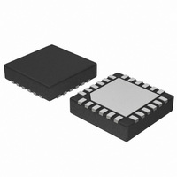
IC EQUALIZER RECEIVER 24-QFN

NB7VQ1006MMNTXG

Manufacturer Part Number
NB7VQ1006MMNTXG
Description
IC EQUALIZER RECEIVER 24-QFN
Manufacturer
ON Semiconductor
Datasheet

Specifications of NB7VQ1006MMNTXG

Logic Type
Equalizer Receiver
Supply Voltage
1.71 V ~ 2.625 V
Number Of Bits
1
Operating Temperature
-40°C ~ 85°C
Mounting Type
Surface Mount
Package / Case
24-TFQFN Exposed Pad
Operating Supply Voltage (min)
1.71V
Operating Supply Voltage (max)
2.625V
Operating Temp Range
-40C to 85C
Operating Temperature Classification
Industrial
Mounting
Surface Mount
Pin Count
24
Supply Voltage (max)
2.625 V
Supply Voltage (min)
1.71 V
Maximum Operating Temperature
+ 85 C
Mounting Style
SMD/SMT
Data Rate
10 Gbps
Minimum Operating Temperature
- 40 C
Supply Current
100 mA, 180 mA
Lead Free Status / RoHS Status
Lead free / RoHS Compliant

Available stocks

Company
Part Number
Manufacturer
Quantity
Price
Part Number:
NB7VQ1006MMNTXG
Manufacturer:
ON/安森美
Quantity:
20 000
NB7VQ1006M
1.8V / 2.5V 10Gbps
Equalizer Receiver with 1:6
Differential CML Outputs
Multi−Level Inputs w/ Internal Termination
Description
fanout buffer with a selectable Equalizer receiver. When placed in
series with a Data path operating up to 10 Gb/s, the NB7VQ1006M
will compensate the degraded data signal transmitted across a FR4
PCB backplane or cable interconnect and output six identical CML
copies of the input signal. Therefore, the serial data rate is increased by
reducing Inter−Symbol Interference (ISI) caused by losses in copper
interconnect or long cables.
flow through or bypass the Equalizer section. Control of the Equalizer
function is realized by setting EQEN; When EQEN is set Low, the
IN/IN inputs bypass the Equalizer. When EQEN is set High, the IN/IN
inputs flow through the Equalizer. The default state at startup is LOW.
As such, the NB7VQ1006M is ideal for SONET, GigE, Fiber Channel,
Backplane and other Data distribution applications.
resistors that are accessed through the VT pin. This feature allows the
NB7VQ1006M to accept various logic level standards, such as
LVPECL, CML or LVDS. This feature provides transmission line
termination at the receiver, eliminating external components. The
outputs have the flexibility of being powered by either a 1.8 V or 2.5 V
supply.
performance Clock/Data products.
Features
*For additional information on our Pb−Free strategy and soldering details, please
© Semiconductor Components Industries, LLC, 2010
June, 2010 − Rev. 2
download the ON Semiconductor Soldering and Mounting Techniques
Reference Manual, SOLDERRM/D.
The NB7VQ1006M is a high performance differential 1:6 CML
The EQualizer ENable pin (EQEN) allows the IN/IN inputs to either
The differential inputs incorporate internal 50 W termination
The NB7VQ1006M is a member of the GigaComm™ family of high
Maximum Input Data Rate > 10 Gbps
Maximum Input Clock Frequency > 7.5 GHz
Backplane and Cable Interconnect Compensation
225 ps Typical Propagation Delay
30 ps Typical Rise and Fall Times
Differential CML Outputs, 400 mV Peak−to−Peak, Typical
Operating Range: V
Internal Input Termination Resistors, 50 W
QFN−24 Package, 4 mm x 4 mm
−40°C to +85°C Ambient Operating Temperature
These are Pb−Free Devices*
CC
= 1.71 V to 2.625 V, GND = 0 V
1
*For additional marking information, refer to
See detailed ordering and shipping information in the package
dimensions section on page 9 of this data sheet.
Application Note AND8002/D.
A
L
Y
W
G
(Note: Microdot may be in either location)
SIMPLIFIED BLOCK DIAGRAM
ORDERING INFORMATION
= Assembly Location
= Wafer Lot
= Year
= Work Week
= Pb−Free Package
http://onsemi.com
MN SUFFIX
CASE 485L
QFN−24
EQ
Publication Order Number:
1
NB7VQ1006M/D
DIAGRAM*
24
MARKING
Q1006M
ALYWG
NB7V
G

Related parts for NB7VQ1006MMNTXG

NB7VQ1006MMNTXG Summary of contents

Page 1

... Ambient Operating Temperature • These are Pb−Free Devices* *For additional information on our Pb−Free strategy and soldering details, please download the ON Semiconductor Soldering and Mounting Techniques Reference Manual, SOLDERRM/D. © Semiconductor Components Industries, LLC, 2010 June, 2010 − Rev. 2 http://onsemi.com QFN− ...

Page 2

Multi−Level Inputs LVPECL, LVDS, CML EQEN (Equalizer Enable Figure 1. Table 1. EQUALIZER ENABLE FUNCTION EQEN 0 1 VCC EQEN VCC Detailed Block Diagram of ...

Page 3

Table 2. PIN DESCRIPTION Pin Name I/O 1 VCC Positive Supply Voltage for the Core Logic 2 IN LVPECL, CML, Non−inverted Differential Clock/Data Input. (Note 1) LVDS Input 3 IN LVPECL, CML, Inverted Differential Clock/Data Input. (Note 1) LVDS Input ...

Page 4

Table 3. ATTRIBUTES ESD Protection Moisture Sensitivity (Note 3) Flammability Rating Transistor Count Meets or exceeds JEDEC Spec EIA/JESD78 IC Latchup Test 3. For additional information, see Application Note AND8003/D. Table 4. MAXIMUM RATINGS Symbol Parameter V , Positive Power ...

Page 5

Table 5. DC CHARACTERISTICS − CML OUTPUT Symbol Characteristic POWER SUPPLY CURRENT (Inputs and Outputs open) I Power Supply Current, Core Logic CC I Power Supply Current, Outputs CCO CML OUTPUTS (Notes 5 and 6) (Figure 10) V Output HIGH ...

Page 6

Table 6. AC CHARACTERISTICS V Symbol f Maximum Operating Input Data Rate DATA f Maximum Input Clock Frequency MAX V Output Voltage Amplitude EQEN = OUTPP (See Figures 4, Note 9) V Input Common Mode Range (Differential ...

Page 7

− IHD(IN) ILD(IN IHD IN V ILD Figure 5. Differential Inputs Driven Differentially CM(MAX CM(MIN) GND Q DUT Driver Device Q Figure 8. Typical Termination for CML Output ...

Page 8

V V CCO GND Figure 9. Typical CML Output Structure and Termination Driver Q Q DJ1 Figure 11. Typical NB7VQ1006 Equalizer Application and Interconnect with PRBS23 pattern at 7.0 Gbps V CCO ...

Page 9

... CML Driver GND Figure 14. Standard 50 W Load CML Interface ORDERING INFORMATION Device NB7VQ1006MMNG NB7VQ1006MMNHTBG NB7VQ1006MMNTXG †For information on tape and reel specifications, including part orientation and tape sizes, please refer to our Tape and Reel Packaging Specifications Brochure, BRD8011/ NB7VQ1006M LVDS Driver GND ...

Page 10

... Opportunity/Affirmative Action Employer. This literature is subject to all applicable copyright laws and is not for resale in any manner. PUBLICATION ORDERING INFORMATION LITERATURE FULFILLMENT: Literature Distribution Center for ON Semiconductor P.O. Box 5163, Denver, Colorado 80217 USA Phone: 303−675−2175 or 800−344−3860 Toll Free USA/Canada Fax: 303− ...

Related keywords