MC14504BDTG ON Semiconductor, MC14504BDTG Datasheet

IC LEVEL SHIFTER HEX 16-TSSOP

MC14504BDTG

Manufacturer Part Number
MC14504BDTG
Description
IC LEVEL SHIFTER HEX 16-TSSOP
Manufacturer
ON Semiconductor
Series
4000Br
Datasheet

Specifications of MC14504BDTG

Logic Function
Level Shifter
Number Of Bits
6
Input Type
TTL, CMOS
Output Type
CMOS
Number Of Channels
6
Number Of Outputs/channel
1
Differential - Input:output
No/No
Propagation Delay (max)
280ns
Voltage - Supply
3 V ~ 18 V
Operating Temperature
-55°C ~ 125°C
Package / Case
16-TSSOP
Supply Voltage
3 V ~ 18 V
Logic Type
Voltage Level Translator
Logic Family
MC145
Translation
CMOS/TTL to CMOS
Input Bias Current (max)
5 mA
High Level Output Current
- 4.2 mA
Low Level Output Current
4.2 mA
Propagation Delay Time
550 ns
Supply Voltage (max)
18 V
Supply Voltage (min)
3 V
Maximum Operating Temperature
+ 125 C
Minimum Operating Temperature
- 55 C
Mounting Style
SMD/SMT
Lead Free Status / RoHS Status
Lead free / RoHS Compliant
Data Rate
-
Lead Free Status / Rohs Status
Lead free / RoHS Compliant
Other names
MC14504BDTG
MC14504BDTGOS
MC14504B
Hex Level Shifter for TTL to
CMOS or CMOS to CMOS
technology. The level shifter will shift a TTL signal to CMOS logic
levels for any CMOS supply voltage between 5 and 15 volts. A control
input also allows interface from CMOS to CMOS at one logic level to
another logic level: Either up or down level translating is
accomplished by selection of power supply levels V
V
voltage levels.
Features
Maximum ratings are those values beyond which device damage can occur.
Maximum ratings applied to the device are individual stress limit values (not
normal operating conditions) and are not valid simultaneously. If these limits are
exceeded, device functional operation is not implied, damage may occur and
reliability may be affected.
1. Temperature Derating:
static voltages or electric fields. However, precautions must be taken to avoid
applications of any voltage higher than maximum rated voltages to this
high−impedance circuit. For proper operation, V
to the range V
either V
MAXIMUM RATINGS
© Semiconductor Components Industries, LLC, 2005
August, 2005 − Rev. 6
Symbol
CC
I
The MC14504B is a hex non−inverting level shifter using CMOS
in
This device contains protection circuitry to guard against damage due to high
Unused inputs must always be tied to an appropriate logic voltage level (e.g.,
from a High to a Low Voltage
or Power Down
Schottky TTL Load Over the Rated Temperature Range
UP Translates from a Low to a High Voltage or DOWN Translates
Input Threshold Can Be Shifted for TTL Compatibility
No Sequencing Required on Power Supplies or Inputs for Power Up
3 to 18 Vdc Operation for V
Diode Protected Inputs to V
Capable of Driving Two Low−Power TTL Loads or One Low−Power
Pb−Free Packages are Available*
V
V
V
T
Plastic “P and D/DW” Packages: – 7.0 mW/_C From 65_C To 125_C
V
P
, I
T
T
stg
CC
DD
out
in
A
D
L
out
level sets the input signal levels while V
SS
or V
DC Supply Voltage Range
Input Voltage Range
(DC or Transient)
Output Voltage Range
(DC or Transient)
Input or Output Current
(DC or Transient) per Pin
Power Dissipation, per Package
(Note 1)
Ambient Temperature Range
Storage Temperature Range
Lead Temperature
(8−Second Soldering)
SS
DD
v (V
). Unused outputs must be left open.
in
Parameter
or V
(Voltages Referenced to V
out
) v V
SS
DD
DD
and V
.
CC
in
and V
−0.5 to V
SS
−0.5 to +18.0
−0.5 to +18.0
−0.5 to +18.0
−55 to +125
−65 to +150
DD
out
)
Value
should be constrained
± 10
500
260
selects the output
DD
DD
and V
+ 0.5
1
CC
Unit
mW
mA
. The
°C
°C
°C
V
V
V
V
See detailed ordering and shipping information in the package
dimensions section on page 2 of this data sheet.
*For additional information on our Pb−Free strategy
and soldering details, please download the
ON Semiconductor Soldering and Mounting
Techniques Reference Manual, SOLDERRM/D.
ORDERING INFORMATION
A
WL, L
YY, Y
WW, W
G
http://onsemi.com
CASE 751B
CASE 948F
SOEIAJ−16
TSSOP−16
DT SUFFIX
CASE 648
CASE 966
P SUFFIX
D SUFFIX
F SUFFIX
PDIP−16
SOIC−16
= Assembly Location
= Wafer Lot
= Year
= Work Week
= Pb−Free Indicator
Publication Order Number:
16
1
16
16
1
1
DIAGRAMS
16
MARKING
MC14504BCP
AWLYYWWG
1
MC14504B
AWLYWW
MC14504B/D
14504BG
ALYWG
ALYW
504B
14

Related parts for MC14504BDTG

MC14504BDTG Summary of contents

Page 1

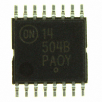
... See detailed ordering and shipping information in the package dimensions section on page 2 of this data sheet. and V should be constrained *For additional information on our Pb−Free strategy in out and soldering details, please download the ON Semiconductor Soldering and Mounting Techniques Reference Manual, SOLDERRM/D. 1 http://onsemi.com MARKING DIAGRAMS 16 PDIP−16 ...

Page 2

PIN ASSIGNMENT out out MODE out out out ...

Page 3

ELECTRICAL CHARACTERISTICS Î Î Î Î Î ...

Page 4

SWITCHING CHARACTERISTICS Î Î Î Î Î ...

Page 5

0.25 (0.010) M −A− −B− −T− SEATING PLANE 0.25 (0.010 MC14504B PACKAGE DIMENSIONS ...

Page 6

K 16X REF 0.10 (0.004) 0.15 (0.006 L PIN 1 IDENT. 1 0.15 (0.006 −V− C 0.10 (0.004) SEATING −T− PLANE D MC14504B PACKAGE DIMENSIONS TSSOP−16 DT SUFFIX PLASTIC TSSOP ...

Page 7

VIEW 0.10 (0.004) 0.13 (0.005) M MC14504B PACKAGE DIMENSIONS SOEIAJ−16 F SUFFIX PLASTIC EIAJ SOIC PACKAGE CASE 966−01 ISSUE ...

Page 8

... Fax: 480−829−7709 or 800−344−3867 Toll Free USA/Canada Email: orderlit@onsemi.com MC14504B N. American Technical Support: 800−282−9855 Toll Free USA/Canada Japan: ON Semiconductor, Japan Customer Focus Center 2−9−1 Kamimeguro, Meguro−ku, Tokyo, Japan 153−0051 Phone: 81−3−5773−3850 http://onsemi.com 8 ON Semiconductor Website: http://onsemi ...

Related keywords