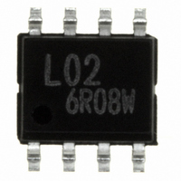
BR24L04F-WE2 Rohm Semiconductor, BR24L04F-WE2 Datasheet

BR24L04F-WE2
Specifications of BR24L04F-WE2
BR24L04F-WE2TR
Available stocks
Related parts for BR24L04F-WE2
BR24L04F-WE2 Summary of contents
Page 1
TECHNICAL NOTE HIGH GRADE Specification HIGH RELIABILITY series HIGH GRADE Specification HIGH RELIABILITY series I C BUS Serial EEPROMs 2 Supply voltage 1.8V~5.5V Operating temperature –40°C~+85°C type BR24L01A-W, BR24L02-W, BR24L04-W, BR24L08-W, BR24L16-W, BR24L32-W, BR24L64-W Description BR24L -W series is a ...
Page 2
... By setting WP "HIGH" in the area, write can be cancelled. When it is set WP = "HIGH" during tWR, write is forcibly ended, and data of address under access is not guaranteed, therefore write it once again Start condition 2/16 Memory cell characteristics (Ta = 25˚C, Vcc = 1.8 ~ 5.5V) Unit Parameter V Min. *2 ...
Page 3
Block diagram * GND 4 Pin assignment and description BR24L01A BR24L02-W BR24L04-W BR24L08 BR24L16-W A2 SCL BR24L32-W BR24L64-W 4 ...
Page 4
Characteristic data 2.5 [BR24L01A/02/04/08/16 series] SPEC 2 f =400kHz SCL DATA=AAh 1.5 Ta=25˚C 1 Ta=85˚C Ta=-40˚C 0 SUPPLY VOLTAGE : V (V) CC Fig.9 Consumption current at write action I (f =400kHz) ...
Page 5
Characteristic data 300 SPEC2 200 SPEC1 : FAST-MODE SPEC2 : STANDARD-MODE SPEC1 100 Ta=85˚C 0 Ta=25˚C Ta=-40˚C -100 -200 SUPPLY VOLTAGE : V (V) CC Fig.24 Input data setup time t (LOW) SU:DAT 5 ...
Page 6
I2C BUS communication BUS data communication BUS data communication starts by start condition input, and ends by stop condition input. Data is always 8bit long, and acknowledge is always required after each byte. I ...
Page 7
... Fig.39 Page write cycle (BR24L32/64-W) Data is written to the address designated by word address (n-th address). By issuing stop bit after 8bit data input, write to memory cell inside starts. When internal write is started, command is not accepted for tWR (5ms at maximum). By page write cycle, the following can be written in bulk bytes (BR24L01A-W, BR24L02-W) And when data of the maximum bytes or higher is sent, data from the first byte is overwritten. (Refer to " ...
Page 8
Notes on write cycle continuous input SLAVE WORD R T ADDRESS (n) T ADDRESS E *1 SDA LINE Note ...
Page 9
Command Read cycle Data of EEPROM is read. In read cycle, there are random read cycle and current read cycle. Random read cycle is a command to read data by designating address, and is used generally. Current read cycle is ...
Page 10
Software reset Software reset is executed when to avoid malfunction after power on, and to reset during command input. Software reset has several kinds, and 3 kinds of them are shown in the figure below. (Refer to Fig. 48 (a), ...
Page 11
WP valid timing (write cancel usually fixed to "H" or "L", but when WP is used to cancel write cycle and so forth, pay attention to the following WP valid timing. During write cycle execution, in cancel valid ...
Page 12
I/O peripheral circuit Pull up resistance of SDA terminal SDA is NMOS open drain, so requires pull up resistance. As for this resistance value (R value from microcontroller and the larger the consumption ...
Page 13
Cautions on microcontroller connection BUS recommended that SDA port is of open drain input /output. However, when to use CMOS input / output of tri state to SDA port, insert a series resistance ...
Page 14
I C BUS input / output circuit Input (A0, A2, SCL) Input / output (SDA) Input (A1, WP) Fig.57 Input pin circuit diagram Fig.58 Input / output pin circuit diagram Fig.59 Input pin circuit diagram 14/16 ...
Page 15
Notes on power ON At power on internal circuit and set, Vcc rises through unstable low voltage area, and IC inside is not completely reset, and malfunction may occur. To prevent this, functions of POR circuit and LVCC ...
Page 16
Selection of order type ROHM type BUS type Operating temperature name −40℃〜+85℃ −40℃〜+125℃ Package specifications SOP8/SOP-J8/SSOP-B8/TSSOP-B8/TSSOP-B8J <External appearance> • SOP8 • SOP-J8 • SSOP-B8 3.0±0.2 4.9±0.2 5.0±0 ...
Page 17
Appendix No technical content pages of this document may be reproduced in any form or transmitted by any means without prior permission of ROHM CO.,LTD. The contents described herein are subject to change without notice. The specifications for the product ...


