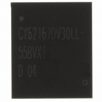
CY62167DV30LL-55BVXI Cypress Semiconductor Corp, CY62167DV30LL-55BVXI Datasheet

CY62167DV30LL-55BVXI
Specifications of CY62167DV30LL-55BVXI
CY62167DV30LL-55BVXI
Available stocks
Related parts for CY62167DV30LL-55BVXI
CY62167DV30LL-55BVXI Summary of contents
Page 1
... Power-Down Note 1. For best-practice recommendations, please refer to the Cypress application note “System Design Guidelines” on http://www.cypress.com. Cypress Semiconductor Corporation Document Number : 38-05328 Rev. *I 16-Mbit (1M x 16) Static RAM also has an automatic power-down feature that significantly reduces power consumption by 99% when addresses are not toggling ...
Page 2
Contents Product Portfolio .............................................................. 3 Pin Configuration ............................................................. 3 Maximum Ratings ............................................................. 4 Operating Range ............................................................... 4 Electrical Characteristics ................................................. 4 Capacitance ...................................................................... 5 Thermal Resistance .......................................................... 5 AC Test Loads and Waveforms ....................................... 5 Data Retention Characteristics ....................................... 5 ...
Page 3
... Product Portfolio V Range (V) CC Product Min Typ CY62167DV30LL 2.2 3.0 Pin Configuration A15 1 A14 2 A13 3 A12 4 A11 5 A10 A19 CE2 12 DNU 13 BHE 14 BLE 15 A18 16 A17 Notes 2. Typical values are included for reference only and are not guaranteed or tested. Typical values are measured ...
Page 4
... Typical values are included for reference only and are not guaranteed or tested. Typical values are measured at V Document Number : 38-05328 Rev. *I Output current into outputs (LOW) .............................. 20 mA Static discharge voltage.......................................... > 2001 V (per MIL-STD-883, Method 3015) Latch-up current ..................................................... > 200 mA Operating Range Device + 0 CY62167DV30LL Industrial + 0 0 Test Conditions = –0 2. ...
Page 5
... Fall Time = 1 V/ns V Unit V [12] Min Typ 1.5 – – – < 0 < 0 – CY62167DV30LL-55 55 – CY62167DV30LL- °C CC CC(typ) A > 100 s. Unit pF pF Unit Max Unit – V A 10 – ns – ns Page ...
Page 6
... HZCE HZBE HZWE 18. The internal Write time of the memory is defined by the overlap of WE, CE and any of these signals can terminate a write by going INACTIVE. The data input set-up and hold timing should be referenced to the edge of the signal that terminates the Write. Document Number : 38-05328 Rev. *I ...
Page 7
Switching Waveforms Figure 2. Read Cycle 1 (Address Transition Controlled) ADDRESS PREVIOUS DATA VALID DATA OUT ADDRESS ACE BHE/BLE t LZBE OE t LZOE HIGH IMPEDANCE DATA OUT t LZCE SUPPLY ...
Page 8
... HZOE Notes 22. The internal Write time of the memory is defined by the overlap of WE write and any of these signals can terminate a write by going INACTIVE. The data input set-up and hold timing should be referenced to the edge of the signal that terminates the Write. 23. Data I/O is high-impedance ...
Page 9
... DATA I/O Note 29 Notes 26. The internal Write time of the memory is defined by the overlap of WE write and any of these signals can terminate a write by going INACTIVE. The data input set-up and hold timing should be referenced to the edge of the signal that terminates the Write. ...
Page 10
Switching Waveforms (continued) Figure 7. Write Cycle 4 (BHE/BLE Controlled, OE LOW) ADDRESS BHE/BLE Note 31 DATA I/O Notes 30 goes HIGH and CE goes LOW simultaneously with ...
Page 11
Truth Table BHE ...
Page 12
... Ordering Information Speed Ordering Code (ns) 55 CY62167DV30LL-55BVI CY62167DV30LL-55BVXI CY62167DV30LL-55ZXI 70 CY62167DV30LL-70BVI Please contact your local Cypress sales representative for availability of these parts Ordering Code Definition CY 621 6 7D Document Number : 38-05328 Rev. *I Package Package Type Diagram 51-85178 48-ball Fine Pitch BGA ( mm) 48-ball Fine Pitch BGA ( ...
Page 13
Package Diagrams Document Number : 38-05328 Rev. *I 48-ball VFBGA ( mm) (51-85178) CY62167DV30 MoBL 51-85178 *A Page ...
Page 14
Document Number : 38-05328 Rev. *I 48-pin TSOP I ( mm) (51-85183) CY62167DV30 MoBL 51-85183 *B Page ...
Page 15
... Acronyms Acronym Description CMOS complementary metal oxide semiconductor I/O input/output SRAM static random access memory VFBGA very fine ball grid array TSOP thin small outline package Document Conventions Units of Measure Symbol Unit of Measure °C degrees Celsius A microamperes mA milliampere MHz megahertz ...
Page 16
Document History Page Document Title: CY62167DV30 MoBL Document Number: 38-05328 REV. ECN NO. Issue Date ** 118408 09/30/02 *A 123692 02/11/03 *B 126555 04/25/03 *C 127841 09/10/03 *D 205701 *E 238050 See ECN *F 304054 See ECN *G 492895 See ...
Page 17
... Use may be limited by and subject to the applicable Cypress software license agreement. Document Number : 38-05328 Rev. *I MoBL is a registered trademark and More Battery Life is a trademark of Cypress Semiconductor Corporation. All product and company names mentioned in this document may be the trademarks of their respective holders. ...


