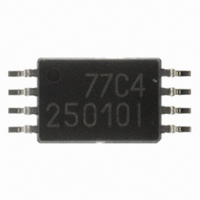
CAT25010YI-GT3 ON Semiconductor, CAT25010YI-GT3 Datasheet

CAT25010YI-GT3
Specifications of CAT25010YI-GT3
CAT25010YI-GT3TR
Available stocks
Related parts for CAT25010YI-GT3
CAT25010YI-GT3 Summary of contents
Page 1
CAT25010, CAT25020, CAT25040 1-Kb, 2-Kb and 4-Kb SPI Serial CMOS EEPROM Description The CAT25010/20/40 are 1−Kb/2−Kb/4−Kb Serial CMOS EEPROM devices internally organized as 128x8/256x8/512x8 bits. They feature a 16−byte page write buffer and support the Serial Peripheral Interface (SPI) protocol. ...
Page 2
Table 1. ABSOLUTE MAXIMUM RATINGS Operating Temperature Storage Temperature Voltage on any Pin with Respect to Ground (Note 1) Stresses exceeding Maximum Ratings may damage the device. Maximum Ratings are stress ratings only. Functional operation above the Recommended Operating Conditions ...
Page 3
Table 5. A.C. CHARACTERISTICS Symbol Parameter f Clock Frequency SCK t Data Setup Time SU t Data Hold Time H t SCK High Time WH t SCK Low Time WL t HOLD to Output Low (Note 5) ...
Page 4
... The BP0 and BP1 (Block Protect) bits determine which blocks are currently write protected. They are set by the user with the WRSR command and are non−volatile. The user is allowed to protect a quarter, one half or the entire memory, by setting these bits according to Table 9. The protected blocks then become read−only. ...
Page 5
... The device contains a Write Enable Latch (WEL) which must be set before attempting to write to the memory array or to the status register. In addition, the address of the memory location( written must be outside the protected area, as defined by BP0 and BP1 bits from the status register. ...
Page 6
Byte Write Once the WEL bit is set, the user may execute a write sequence, by sending a WRITE instruction, a 8−bit address and data as shown in Figure 5. For the CAT25040, bit 3 of the write instruction opcode ...
Page 7
... WP Dashed Line = mode (1, 1) Write Protection When WP input is low all write operations to the memory array and Status Register are inhibited. WP going low while CS is still low will interrupt a write to the status register. If the internal write cycle has already been initiated, WP going low will have no effect on any write operation to the Status Register ...
Page 8
... Read from Memory Array To read from memory, the host sends a READ instruction followed by a 8−bit address (for the CAT25040, bit 3 of the read instruction opcode contains A8 address bit). After receiving the last address bit, the CAT25010/20/40 will respond by shifting out data on the SO pin (as shown in Figure 9) ...
Page 9
... The CS input must be set high after the proper number of clock cycles to start the internal write cycle. Access to the memory array during an internal write cycle is ignored and programming is continued. Any invalid exceeds the POR op− ...
Page 10
PIN # 1 IDENTIFICATION D TOP VIEW SIDE VIEW Notes: (1) All dimensions are in millimeters. (2) Complies with JEDEC MS-001. PACKAGE DIMENSIONS PDIP−8, 300 mils CASE 646AA−01 ISSUE A SYMBOL ...
Page 11
PIN # 1 IDENTIFICATION TOP VIEW SIDE VIEW Notes: (1) All dimensions are in millimeters. Angles in degrees. (2) Complies with JEDEC MS-012. PACKAGE DIMENSIONS SOIC 8, 150 mils CASE 751BD−01 ISSUE O SYMBOL ...
Page 12
E1 e TOP VIEW SIDE VIEW Notes: (1) All dimensions are in millimeters. Angles in degrees. (2) Complies with JEDEC MO-153. PACKAGE DIMENSIONS TSSOP8, 4.4x3 CASE 948AL−01 ISSUE O SYMBOL MIN A A1 0.05 A2 ...
Page 13
D E PIN#1 INDEX AREA TOP VIEW SYMBOL MIN NOM A 0.70 0.75 A1 0.00 0.02 A2 0.45 0.55 A3 0.20 REF b 0.20 0.25 D 1.90 2.00 D2 1.30 1.40 E 2.90 3.00 E2 1.20 1.30 e 0.50 TYP ...
Page 14
E E1 TOP VIEW SIDE VIEW Notes: (1) All dimensions are in millimeters. Angles in degrees. (2) Complies with JEDEC MO-187. PACKAGE DIMENSIONS MSOP 8, 3x3 CASE 846AD−01 ISSUE O SYMBOL MIN A A1 ...
Page 15
... For MSOP package availability, please contact your nearest ON Semiconductor Sales office. 14. For additional package and temperature options, please contact your nearest ON Semiconductor Sales office. 15. For information on tape and reel specifications, including part orientation and tape sizes, please refer to our Tape and Reel Packaging Specifications Brochure, BRD8011/D ...


