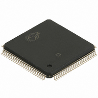
CY7C09389V-12AXC Cypress Semiconductor Corp, CY7C09389V-12AXC Datasheet

CY7C09389V-12AXC
Specifications of CY7C09389V-12AXC
Available stocks
Related parts for CY7C09389V-12AXC
CY7C09389V-12AXC Summary of contents
Page 1
... A –A for 32K; A –A for 64K devices Cypress Semiconductor Corporation Document #: 38-06056 Rev. *C 3.3V 16K/32K/64K x 16/18 Synchronous Dual-Port Static RAM ■ 3.3V low operating power: ❐ Active = 115 mA (typical) Standby = 10 μA (typical) ❐ ■ Fully synchronous interface for easier operation ■ ...
Page 2
Pinouts 100 A9L 1 A10L 2 A11L 3 A12L 4 A13L 5 A14L 6 [6] [7] A15L LBL 10 UBL 11 CE0L 12 CE1L 13 CNTRSTL 14 VCC 15 R/WL 16 OEL ...
Page 3
... SB3 (Both Ports CMOS Level) Notes 9. This pin is NC for CY7C09369V. 10. This pin is NC for CY7C09369V and CY7C09379V. Document #: 38-06056 Rev. *C Figure 2. 100-Pin TQFP (Top View CY7C09389V (64K x 18) CY7C09379V (32K x 18) CY7C09369V (16K x 18 CY7C09269V/79V/89V CY7C09369V/79V/89V [1, 2] [2] -7 100 83 6 ...
Page 4
... Output Enable Input. This signal must be asserted LOW to enable the I/O data pins during read L R operations. R/W R/W Read/Write Enable Input. This signal is asserted LOW to write to the dual port memory array. For L R read operations, assert this pin HIGH. FT/PIPE FT/PIPE Flow Through/Pipelined Select Input ...
Page 5
Maximum Ratings [12] Exceeding maximum ratings may impair the useful life of the device. These user guidelines are not tested. Storage Temperature ..................................... −65°C to +150°C Ambient Temperature with Power Applied.................................................. −55°C to +125°C Supply Voltage to Ground Potential .................−0.5V ...
Page 6
R1 = 590Ω OUTPUT 435Ω (a) Normal Load (Load 1) Figure 4. AC Test Loads (Applicable to -6 and -7 only 50Ω 50Ω 0 OUTPUT C (a) Load 1 ...
Page 7
Switching Characteristics Over the Operating Range Parameter Description f f Flow Through MAX1 Max f f Pipelined MAX2 Max t Clock Cycle Time - Flow Through CYC1 t Clock Cycle Time - Pipelined CYC2 t Clock HIGH Time - Flow ...
Page 8
Switching Waveforms Figure 5. Read Cycle for Flow Through Output (FT/PIPE = V t CYC1 t CH1 CLK R ADDRESS t CD1 ...
Page 9
Switching Waveforms (continued) t CYC2 t t CH2 CL2 CLK ADDRESS A (B1 0(B1) DATA OUT(B1 ADDRESS A (B2 0(B2 ...
Page 10
... OE Notes 27. Output state (High, LOW, or high impedance) is determined by the previous cycle control signals. 28. CE and ADS = CNTEN, and CNTRST = 29. During “No Operation”, data in memory at the selected address may be corrupted and must be rewritten to ensure data integrity. Document #: 38-06056 Rev n+1 n+2 ...
Page 11
Switching Waveforms (continued) Figure 11. Flow Through Read-to-Write-to-Read ( CYC1 t t CH1 CL1 CLK R ADDRESS DATA IN ...
Page 12
Switching Waveforms (continued) Figure 13. Pipelined Read with Address Counter Advance t CYC2 t t CH2 CL2 CLK ADDRESS SAD HAD ADS CNTEN t t SCN HCN DATA OUT Q x-1 READ ...
Page 13
Switching Waveforms (continued) Figure 15. Write with Address Counter Advance (Flow Through or Pipelined Outputs) t CYC2 t t CH2 CL2 CLK ADDRESS n INTERNAL A n ADDRESS t t SAD HAD ADS CNTEN t ...
Page 14
Switching Waveforms (continued) Figure 16. Counter Reset (Pipelined Outputs) t CYC2 t t CH2 CL2 CLK ADDRESS INTERNAL A X ADDRESS SAD HAD ADS t t SCN HCN CNTEN t t SRST HRST CNTRST t ...
Page 15
Read/Write and Enable Operation Inputs OE CLK Address Counter Control Operation Previous Address CLK ADS Address ...
Page 16
Ordering Information 16K x16 3.3V Synchronous Dual-Port SRAM Speed (ns) Ordering Code [1, 2] 6.5 CY7C09269V-6AC CY7C09269V-6AXC [2] 7.5 CY7C09269V-7AC CY7C09269V-7AXC 9 CY7C09269V-9AC CY7C09269V-9AXC CY7C09269V-9AI 12 CY7C09269V-12AC CY7C09269V-12AXC 32K x16 3.3V Synchronous Dual-Port SRAM Speed (ns) Ordering Code [1, 2] ...
Page 17
... CY7C09389V-7AC CY7C09389V-7AXC 9 CY7C09389V-9AC CY7C09389V-9AXC CY7C09389V-9AI CY7C09389V-9AXI 12 CY7C09389V-12AC CY7C09389V-12AXC Document #: 38-06056 Rev. *C Package Package Type Diagram 51-85048 100-Pin Thin Quad Flat Pack 100-Pin Thin Quad Flat Pack (Pb-Free) 51-85048 100-Pin Thin Quad Flat Pack 100-Pin Thin Quad Flat Pack (Pb-Free) 51-85048 ...
Page 18
Package Diagrams Figure 17. 100-Pin Thin Plastic Quad Flat Pack (TQFP), 51-85048 Document #: 38-06056 Rev. *C CY7C09269V/79V/89V CY7C09369V/79V/89V 51-85048 *C Page [+] Feedback [+] Feedback ...
Page 19
... Cypress against all charges. Any Source Code (software and/or firmware) is owned by Cypress Semiconductor Corporation (Cypress) and is protected by and subject to worldwide patent protection (United States and foreign), United States copyright laws and international treaty provisions. Cypress hereby grants to licensee a personal, non-exclusive, non-transferable license to copy, use, modify, create derivative works of, and compile the Cypress Source Code and derivative works for the sole purpose of creating custom software and or firmware in support of licensee product to be used only in conjunction with a Cypress integrated circuit as specified in the applicable agreement ...


