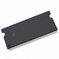
MT48LC2M32B2P-5:G Micron Technology Inc, MT48LC2M32B2P-5:G Datasheet - Page 10

MT48LC2M32B2P-5:G
Manufacturer Part Number
MT48LC2M32B2P-5:G
Description
IC SDRAM 64MBIT 200MHZ 86TSOP
Manufacturer
Micron Technology Inc
Type
SDRAMr
Datasheet
1.MT48LC2M32B2P-6G_TR.pdf
(69 pages)
Specifications of MT48LC2M32B2P-5:G
Format - Memory
RAM
Memory Type
SDRAM
Memory Size
64M (2Mx32)
Speed
200MHz
Interface
Parallel
Voltage - Supply
3 V ~ 3.6 V
Operating Temperature
0°C ~ 70°C
Package / Case
86-TSOP
Organization
2Mx32
Density
64Mb
Address Bus
13b
Access Time (max)
4.5ns
Maximum Clock Rate
200MHz
Operating Supply Voltage (typ)
3.3V
Package Type
TSOP-II
Operating Temp Range
0C to 70C
Operating Supply Voltage (max)
3.6V
Operating Supply Voltage (min)
3V
Supply Current
280mA
Pin Count
86
Mounting
Surface Mount
Operating Temperature Classification
Commercial
Package
86TSOP-II
Address Bus Width
13 Bit
Operating Supply Voltage
3.3 V
Maximum Random Access Time
4.5 ns
Lead Free Status / RoHS Status
Lead free / RoHS Compliant
Table 4:
Functional Description
Initialization
PDF: 09005aef811ce1fe/Source: 09005aef811ce1d5
64MSDRAMx32_2.fm - Rev. J 12/08 EN
3, 9, 35, 41, 49,
14, 21, 30, 57,
46, 52, 78, 84
44, 58, 72, 86
86-Pin TSOP
6, 12, 32, 38,
1, 15, 29, 43
Numbers
55, 75, 81
69, 70, 73
Pin/Ball Descriptions (continued)
90-Ball VFBGA
E1, L1, M9, N9,
E9, L9, M1, N1,
B2, B7, C9, D9,
B8, B3, C1, D1,
E3, E7, H3, H7,
A7, F9, L7, R7
A3, F1, L3, R3
K2, K3, H9
Numbers
P2, P7
P3, P8
In general, this 64Mb SDRAM (512K x 32 x 4 banks) is a 4-bank DRAM that operates at
3.3V and includes a synchronous interface (all signals are registered on the positive edge
of the clock signal, CLK). Each of the 16,777,216-bit banks is organized as 2,048 rows by
256 columns by 32 bits.
Read and write accesses to the SDRAM are burst oriented; accesses start at a selected
location and continue for a programmed number of locations in a programmed
sequence. Accesses begin with the registration of an ACTIVE command, which is then
followed by a READ or WRITE command. The address bits registered coincident with the
ACTIVE command are used to select the bank and row to be accessed (BA0 and BA1
select the bank, A0–A10 select the row). The address bits (A0–A7) registered coincident
with the READ or WRITE command are used to select the starting column location for
the burst access.
Prior to normal operation, the SDRAM must be initialized. The following sections
provide detailed information covering device initialization, register definition,
command descriptions, and device operation.
SDRAMs must be powered up and initialized in a predefined manner. Operational
procedures other than those specified may result in undefined operation. After power is
applied to V
defined as a signal cycling within timing constraints specified for the clock pin), the
SDRAM requires a 100µs delay prior to issuing any command other than a COMMAND
INHIBIT or NOP. Starting at some point during this 100µs period, and continuing at least
through the end of this period, COMMAND INHIBIT or NOP commands must be
applied.
When the 100µs delay has been satisfied with at least one COMMAND INHIBIT or NOP
command having been applied, a PRECHARGE command should be applied. All banks
must then be precharged, thereby placing the device in the all banks idle state.
Symbol
V
V
V
V
DD
NC
SS
DD
SS
Q
Q
DD
and V
Supply
Supply
Supply
Supply
Type
–
DD
Q (simultaneously) and the clock is stable (stable clock is
DQ power supply: Isolated on the die for improved noise
immunity.
DQ ground: Provide isolated ground to DQs for improved noise
immunity.
Power supply: +3.3V ±0.3V. (See note 27 on page 50.)
Ground.
No connect: These pins/balls should be left unconnected. Pin 70
is reserved for SSTL reference voltage supply. H7 is a no connect
for this part but may be used as A12 in future designs. H9 is used
as A11 in 128Mb, 256Mb, and 512Mb x32 FBGAs. PCB designs
that accommodate different densities must account for A11 with
stuffing options.
10
Micron Technology, Inc., reserves the right to change products or specifications without notice.
Description
Functional Description
©2001 Micron Technology, Inc. All rights reserved.
64Mb: x32 SDRAM


