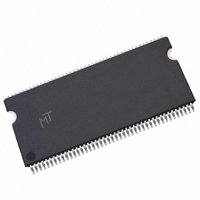
MT48LC2M32B2P-5:G Micron Technology Inc, MT48LC2M32B2P-5:G Datasheet - Page 11

MT48LC2M32B2P-5:G
Manufacturer Part Number
MT48LC2M32B2P-5:G
Description
IC SDRAM 64MBIT 200MHZ 86TSOP
Manufacturer
Micron Technology Inc
Type
SDRAMr
Datasheet
1.MT48LC2M32B2P-6G_TR.pdf
(69 pages)
Specifications of MT48LC2M32B2P-5:G
Format - Memory
RAM
Memory Type
SDRAM
Memory Size
64M (2Mx32)
Speed
200MHz
Interface
Parallel
Voltage - Supply
3 V ~ 3.6 V
Operating Temperature
0°C ~ 70°C
Package / Case
86-TSOP
Organization
2Mx32
Density
64Mb
Address Bus
13b
Access Time (max)
4.5ns
Maximum Clock Rate
200MHz
Operating Supply Voltage (typ)
3.3V
Package Type
TSOP-II
Operating Temp Range
0C to 70C
Operating Supply Voltage (max)
3.6V
Operating Supply Voltage (min)
3V
Supply Current
280mA
Pin Count
86
Mounting
Surface Mount
Operating Temperature Classification
Commercial
Package
86TSOP-II
Address Bus Width
13 Bit
Operating Supply Voltage
3.3 V
Maximum Random Access Time
4.5 ns
Lead Free Status / RoHS Status
Lead free / RoHS Compliant
PDF: 09005aef811ce1fe/Source: 09005aef811ce1d5
64MSDRAMx32_2.fm - Rev. J 12/08 EN
Note:
10. Issue an AUTO REFRESH command.
11. Wait at least
12. The SDRAM is now ready for mode register programming. Because the mode register
13. Wait at least
1. Simultaneously apply power to V
2. Assert and hold CKE at a LVTTL logic LOW since all inputs and outputs are LVTTL-
3. Provide stable CLOCK signal. Stable clock is defined as a signal cycling within timing
4. Wait at least 100µs prior to issuing any command other than a COMMAND INHIBIT
5. Starting at some point during this 100µs period, bring CKE HIGH. Continuing at least
6. Perform a PRECHARGE ALL command.
7. Wait at least
8. Issue an AUTO REFRESH command.
9. Wait at least
When in the idle state, at least two AUTO REFRESH cycles must be performed. After the
AUTO REFRESH cycles are complete, the SDRAM is ready for mode register program-
ming. Because the mode register will power up in an unknown state, it must be loaded
prior to applying any operational command. If desired, the two AUTO REFRESH
commands can be issued after the LOAD MODE REGISTER command.
The recommended power-up sequence for SDRAMs:
At this point the DRAM is ready for any valid command.
compatible.
constraints specified for the clock pin.
or NOP.
through the end of this period, 1 or more COMMAND INHIBIT or NOP commands
must be applied.
given. All banks will complete their precharge, thereby placing the device in the all
banks idle state.
are allowed.
are allowed.
will power up in an unknown state, it should be loaded with desired bit values prior to
applying any operational command. Using the LMR command, program the mode
register. The mode register is programmed via the MODE REGISTER SET command
with BA1 = 0, BA0 = 0 and retains the stored information until it is programmed again
or the device loses power. Not programming the mode register upon initialization will
result in default settings which may not be desired. Outputs are guaranteed High-Z
after the LMR command is issued. Outputs should be High-Z already before the LMR
command is issued.
allowed.
If desired, more than two AUTO REFRESH commands can be issued in the sequence.
After steps 9 and 10 are complete, repeat them until the desired number of AUTO
REFRESH +
t
t
t
t
t
RFC loops is achieved.
RP time; during this time,0 NOPs or DESELECT commands must be
RFC time, during which only NOPs or COMMAND INHIBIT commands
RFC time, during which only NOPs or COMMAND INHIBIT commands
MRD time, during which only NOP or DESELECT commands are
11
DD
and V
Micron Technology, Inc., reserves the right to change products or specifications without notice.
DD
Q.
Functional Description
©2001 Micron Technology, Inc. All rights reserved.
64Mb: x32 SDRAM


