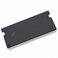
MT48LC2M32B2P-5:G Micron Technology Inc, MT48LC2M32B2P-5:G Datasheet - Page 16

MT48LC2M32B2P-5:G
Manufacturer Part Number
MT48LC2M32B2P-5:G
Description
IC SDRAM 64MBIT 200MHZ 86TSOP
Manufacturer
Micron Technology Inc
Type
SDRAMr
Datasheet
1.MT48LC2M32B2P-6G_TR.pdf
(69 pages)
Specifications of MT48LC2M32B2P-5:G
Format - Memory
RAM
Memory Type
SDRAM
Memory Size
64M (2Mx32)
Speed
200MHz
Interface
Parallel
Voltage - Supply
3 V ~ 3.6 V
Operating Temperature
0°C ~ 70°C
Package / Case
86-TSOP
Organization
2Mx32
Density
64Mb
Address Bus
13b
Access Time (max)
4.5ns
Maximum Clock Rate
200MHz
Operating Supply Voltage (typ)
3.3V
Package Type
TSOP-II
Operating Temp Range
0C to 70C
Operating Supply Voltage (max)
3.6V
Operating Supply Voltage (min)
3V
Supply Current
280mA
Pin Count
86
Mounting
Surface Mount
Operating Temperature Classification
Commercial
Package
86TSOP-II
Address Bus Width
13 Bit
Operating Supply Voltage
3.3 V
Maximum Random Access Time
4.5 ns
Lead Free Status / RoHS Status
Lead free / RoHS Compliant
Operating Mode
Write Burst Mode
Commands
Table 7:
PDF: 09005aef811ce1fe/Source: 09005aef811ce1d5
64MSDRAMx32_2.fm - Rev. J 12/08 EN
Name (Function)
COMMAND INHIBIT (NOP)
NO OPERATION (NOP)
ACTIVE (Select bank and activate row)
READ (Select bank and column, and start READ
burst)
WRITE (Select bank and column, and start WRITE
burst)
BURST TERMINATE
PRECHARGE (Deactivate row in bank or banks)
AUTO REFRESH or SELF REFRESH (Enter self refresh
mode)
LOAD MODE REGISTER
WRITE ENABLE/OUTPUT ENABLE
WRITE INHIBIT/OUTPUT HIGH-Z
Truth Table 1 – Commands and DQM Operation
CKE is HIGH for all commands shown except SELF REFRESH
Notes:
The normal operating mode is selected by setting M7 and M8 to zero; other combina-
tions of values for M7 and M8 are reserved for future use and/or test modes. The
programmed burst length applies to both read and write bursts.
Test modes and reserved states should not be used because unknown operation or
incompatibility with future versions may result.
When M9 = 0, the burst length programmed via M0–M2 applies to both read and write
bursts; when M9 = 1, the programmed burst length applies to read bursts, but write
accesses are single-location (nonburst) accesses.
Truth Table 1 provides a quick reference of available commands. This is followed by a
written description of each command. Three additional Truth Tables appear following
“Operations” on page 19; these tables provide current state/next state information.
1. A0–A10 provide row address, BA0 and BA1 determine which bank is made active.
2. A0–A7 provide column address; A10 HIGH enables the auto precharge feature (nonpersis-
3. A10 LOW: BA0 and BA1 determine the bank being precharged. A10 HIGH: all banks pre-
4. This command is AUTO REFRESH if CKE is HIGH; SELF REFRESH if CKE is LOW.
5. Internal refresh counter controls row addressing; all inputs and I/Os are “Don’t Care” except
6. A0–A10 define the op-code written to the mode register.
7. Activates or deactivates the DQs during WRITEs (zero-clock delay) and READs (two-clock
tent), while A10 LOW disables the auto precharge feature; BA0 and BA1 determine which
bank is being read from or written to.
charged and BA0 and BA1 are “Don’t Care.”
for CKE.
delay). DQM0 controls DQ0–DQ7; DQM1 controls DQ8–DQ15; DQM2 controls DQ16–DQ23;
and DQM3 controls DQ24–DQ31.
CS#
H
L
L
L
L
L
L
L
–
–
L
16
RAS# CAS#
H
H
H
H
X
L
L
L
L
–
–
Micron Technology, Inc., reserves the right to change products or specifications without notice.
X
H
H
H
H
L
L
L
L
–
–
WE#
X
H
H
H
H
L
L
L
L
–
–
DQM
L/H
L/H
X
X
X
X
X
X
X
H
L
7
7
Bank/row
Bank/col
Bank/col
Op-code
©2001 Micron Technology, Inc. All rights reserved.
ADDR
Code
64Mb: x32 SDRAM
X
X
X
X
–
–
High-Z
Active
Active
Valid
Commands
DQs
X
X
X
X
X
X
X
Notes
4, 5
1
2
2
3
6
7
7


