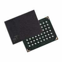
MT45W1MW16PDGA-70 IT TR Micron Technology Inc, MT45W1MW16PDGA-70 IT TR Datasheet - Page 9

MT45W1MW16PDGA-70 IT TR
Manufacturer Part Number
MT45W1MW16PDGA-70 IT TR
Description
IC PSRAM 16MBIT 70NS 48VFBGA
Manufacturer
Micron Technology Inc
Datasheet
1.MT45W1MW16PDGA-70_IT_TR.pdf
(29 pages)
Specifications of MT45W1MW16PDGA-70 IT TR
Format - Memory
RAM
Memory Type
PSRAM (Page)
Memory Size
16M (1M x 16)
Speed
70ns
Interface
Parallel
Voltage - Supply
1.7 V ~ 1.95 V
Operating Temperature
-40°C ~ 85°C
Package / Case
48-VFBGA
Operating Temperature (max)
85C
Operating Temperature (min)
-40C
Mounting
Surface Mount
Operating Temperature Classification
Industrial
Lead Free Status / RoHS Status
Lead free / RoHS Compliant
Functional Description
Power-Up Initialization
Figure 4:
Bus Operating Modes
Asynchronous Mode
PDF: 09005aef81cadc83/Source:09005aef81c6edb4
16mb_asyncpage_cr1_0_p23z_2.fm - Rev. F 4/08 EN
Power-Up Initialization Timing
In general, the MT45W1MW16PD device is a high-density alternative to SRAM and
Pseudo SRAM products, popular in low-power, portable applications. The
MT45W1MW16PD contains a 16,777,216-bit DRAM core organized as 1,048,576
addresses by 16 bits. These devices include the industry-standard, asynchronous mem-
ory interface found on other low-power SRAM or Pseudo SRAM offerings. Page mode
accesses are also included as a bandwidth-enhancing extension to the asynchronous read
protocol.
CellularRAM products include an on-chip voltage sensor that is used to launch the
power-up initialization process. Initialization will load the CR with its default setting.
V
1.7V, the device will require 150µs to complete its self-initialization process (see
Figure 4). During the initialization period, CE# should remain HIGH. When initialization
is complete, the device is ready for normal operation.
Vcc, VccQ = 1.7V
The MT45W1MW16PD CellularRAM product incorporates the industry-standard, asyn-
chronous interface found on other low-power SRAM or Pseudo SRAM offerings. This bus
interface supports asynchronous READ and WRITE operations as well as the band-
width-enhancing page mode READ operation. The specific interface that is supported is
defined by the value loaded into the CR.
CellularRAM products power up in the asynchronous operating mode. This mode uses
the industry-standard SRAM control interface (CE#, OE#, WE#, LB#/UB#). READ opera-
tions (Figure 5) are initiated by bringing CE#, OE#, and LB#/UB# LOW while keeping
WE# HIGH. Valid data will be driven out of the I/Os after the specified access time has
elapsed. WRITE operations (Figure 6) occur when CE#, WE#, and LB#/UB# are driven
LOW. During WRITE operations, the level of OE# is a “Don't Care”; WE# will override
OE#. The data to be written will be latched on the rising edge of CE#, WE#, or LB#/UB#
(whichever occurs first). WE# LOW time must be limited to
CC
and V
CC
Q must be applied simultaneously, and when they reach a stable level above
16Mb: 1 Meg x 16 Async/Page CellularRAM 1.0 Memory
t PU
9
Micron Technology, Inc., reserves the right to change products or specifications without notice.
normal operation
Device ready for
Vcc (MIN)
Functional Description
t
CEM.
©2005 Micron Technology, Inc. All rights reserved.


