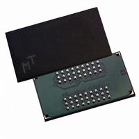
MT48V8M16LFB4-8:G Micron Technology Inc, MT48V8M16LFB4-8:G Datasheet - Page 15

MT48V8M16LFB4-8:G
Manufacturer Part Number
MT48V8M16LFB4-8:G
Description
IC SDRAM 128MBIT 125MHZ 54VFBGA
Manufacturer
Micron Technology Inc
Type
Mobile SDRAMr
Specifications of MT48V8M16LFB4-8:G
Format - Memory
RAM
Memory Type
Mobile SDRAM
Memory Size
128M (8Mx16)
Speed
125MHz
Interface
Parallel
Voltage - Supply
2.3 V ~ 2.7 V
Operating Temperature
0°C ~ 70°C
Package / Case
54-VFBGA
Organization
8Mx16
Density
128Mb
Address Bus
14b
Access Time (max)
19/8/7ns
Maximum Clock Rate
125MHz
Operating Supply Voltage (typ)
2.5V
Package Type
VFBGA
Operating Temp Range
0C to 70C
Operating Supply Voltage (max)
2.7V
Operating Supply Voltage (min)
2.3V
Supply Current
100mA
Pin Count
54
Mounting
Surface Mount
Operating Temperature Classification
Commercial
Lead Free Status / RoHS Status
Lead free / RoHS Compliant
Available stocks
Company
Part Number
Manufacturer
Quantity
Price
Company:
Part Number:
MT48V8M16LFB4-8:G
Manufacturer:
MICRON
Quantity:
4 000
Company:
Part Number:
MT48V8M16LFB4-8:G
Manufacturer:
Micron Technology Inc
Quantity:
10 000
Company:
Part Number:
MT48V8M16LFB4-8:G TR
Manufacturer:
Micron Technology Inc
Quantity:
10 000
Functional Description
Initialization
PDF: 09005aef807f4885/Source: 09005aef8071a76b
128Mbx16x32Mobile_2.fm - Rev. M 1/09 EN
1. Simultaneously apply power to V
2. Assert and hold CKE at a LVTTL logic LOW.
3. Provide stable CLOCK signal. Stable clock is defined as a signal cycling within timing
4. Wait at least 100µs prior to issuing any command other than a COMMAND INHIBIT
5. Starting at some point during this 100µs period, bring CKE HIGH. Continuing at least
6. Perform a PRECHARGE ALL command.
In general, the 128Mb SDRAMs (2 Meg x 16 x 4 banks and 1 Meg x 32 x 4 banks) are quad-
bank DRAMs that operate at 3.3V or 2.5V and include a synchronous interface (all
signals are registered on the positive edge of the clock signal, CLK). Each of the x16’s
33,554,432-bit banks is organized as 4,096 rows by 512 columns by 16 bits. Each of the
x32’s 33,554,432-bit banks is organized as 4,096 rows by 256 columns by 32 bits.
Read and write accesses to the SDRAM are burst oriented; accesses start at a selected
location and continue for a programmed number of locations in a programmed
sequence. Accesses begin with the registration of an ACTIVE command, which is then
followed by a READ or WRITE command. The address bits registered coincident with the
ACTIVE command are used to select the bank and row to be accessed (BA0 and BA1
select the bank, A0–A11 select the row). The address bits (x16: A0–A8; x32: A0–A7) regis-
tered coincident with the READ or WRITE command are used to select the starting
column location for the burst access.
Prior to normal operation, the SDRAM must be initialized. The following sections
provide detailed information covering device initialization, register definition,
command descriptions, and device operation.
SDRAMs must be powered up and initialized in a predefined manner. Operational
procedures other than those specified may result in undefined operation. After power is
applied to V
defined as a signal cycling within timing constraints specified for the clock pin), the
SDRAM requires a 100µs delay prior to issuing any command other than a COMMAND
INHIBIT or NOP . Starting at some point during this 100µs period and continuing at least
through the end of this period, COMMAND INHIBIT or NOP commands must be
applied.
After the 100µs delay has been satisfied with at least one COMMAND INHIBIT or NOP
command having been applied, a PRECHARGE command should be applied. All banks
must then be precharged, thereby placing the device in the all banks idle state.
Once in the idle state, at least two AUTO REFRESH cycles must be performed. After the
AUTO REFRESH cycles are complete, the SDRAM is ready for mode register program-
ming. Because the mode register will power up in an unknown state, it must be loaded
prior to applying any operational command. If desired, the two AUTO REFRESH
commands can be issued after the LOAD MODE REGISTER (LMR) command.
The recommended power-up sequence for SDRAMs:
constraints specified for the clock pin.
or NOP.
through the end of this period, one or more COMMAND INHIBIT or NOP commands
must be applied.
DD
and V
DD
Q (simultaneously) and the clock is stable (stable clock is
15
DD
and V
Micron Technology, Inc., reserves the right to change products or specifications without notice.
DD
128Mb: x16, x32 Mobile SDRAM
Q.
Functional Description
©2001 Micron Technology, Inc. All rights reserved.


