CY7C1049DV33-10VXIT Cypress Semiconductor Corp, CY7C1049DV33-10VXIT Datasheet
CY7C1049DV33-10VXIT
Specifications of CY7C1049DV33-10VXIT
Available stocks


Related parts for CY7C1049DV33-10VXIT


CY7C1049DV33-10VXIT Summary of contents
Page 1
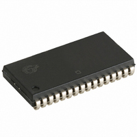
... HIGH), the outputs are disabled (OE HIGH), or during a write operation (CE LOW, and WE LOW). The CY7C1049DV33 is available in standard 400 Mil wide 36 -pin SOJ package and 44-pin TSOP II package with center power and ground (revolutionary) pinout. Refer to the Cypress application note Guidelines for best practice recommendations ...
Page 2
... Pin Configuration 36-Pin SOJ Top View GND Selection Guide Maximum Access Time Maximum Operating Current Maximum CMOS Standby Current Note 1. Automotive product information is preliminary. Document Number: 38-05475 Rev. *F 44-Pin TSOP II Top View GND -10 (Industrial) -12 (Automotive CY7C1049DV33 [1] Unit Page [+] Feedback ...
Page 3
... IN IL MAX Max > V – 0.3V > V – 0.3V < 0.3V Test Conditions T = 25 MHz CY7C1049DV33 Ambient Temperature V Speed CC 3.3V 0.3V –40C to +85 3.3V 0.3V –40C to +125 -10 (Industrial) -12 (Automotive) Max Min Max 2.4 0.4 0 ...
Page 4
... DATA RETENTION MODE 3.0V V > CDR Figure 1. High Z characteristics are tested for all speeds using the test load shown in > 50 s or stable at V > 50 CC(min.) CC(min.) CY7C1049DV33 SOJ TSOP II Package Package Unit C/W 57.91 50.66 C/W 36.73 17.17 [4] ALL INPUT PULSES 90% ...
Page 5
... The minimum write cycle time for Write Cycle No. 2 (WE controlled, OE LOW) is the sum of t Document Number: 38-05475 Rev. *F -10 (Industrial) Min 100 values until the first memory access is performed less than less than t , and t is less than t LZCE HZOE LZOE HZWE and t HZWE CY7C1049DV33 -12 (Automotive) Max Min Max Unit 100 ...
Page 6
... If CE goes HIGH simultaneously with WE going HIGH, the output remains in a high impedance state. Document Number: 38-05475 Rev. *F [13, 14] Figure 3. Read Cycle No OHA DOE DATA VALID 50 SCE PWE t SD DATA VALID IN CY7C1049DV33 DATA VALID [14, 15] t HZOE t HZCE HIGH IMPEDANCE 50 [16, 17 Page [+] Feedback ...
Page 7
... Figure 7. Write Cycle No. 3 (CE Controlled) ADDRESS CE WE DATA I/O Note 18. During this period the IOs are in the output state and input signals must not be applied. Document Number: 38-05475 Rev SCE PWE t SD DATA VALID SCE SCE PWE t SD DATA VALID CY7C1049DV33 [17 LZWE [16, 17 Page [+] Feedback ...
Page 8
... Package Type: xxx = VX or ZSX VX = 36-pin (400-Mil) Molded SOJ (Pb-free) ZSX = 44-pin TSOP II (Pb-free) Speed V33 = Voltage range ( 3 C9 Technology 9 = Data width × 8-bits 04 = 4-Mbit density 1 = Fast Asynchronous SRAM family Technology Code CMOS 7 = SRAM CY = Cypress CY7C1049DV33 Mode Power Standby ( Active ( Active ( ...
Page 9
... Package Diagrams Figure 8. 36-Pin (400-Mil) Molded SOJ (51-85090) Document Number: 38-05475 Rev. *F CY7C1049DV33 51-85090 *E Page [+] Feedback ...
Page 10
... Package Diagrams (continued) Figure 9. 44-Pin Thin Small Outline Package Type II (51-85087) Document Number: 38-05475 Rev. *F CY7C1049DV33 51-85087 *C Page [+] Feedback ...
Page 11
... Document History Page Document Title: CY7C1049DV33, 4-Mbit (512K x 8) Static RAM Document Number: 38-05475 Orig. of REV. ECN NO. Issue Date Change ** 201560 See ECN SWI *A 233729 See ECN SYT *B 351096 See ECN PCI *C 446328 See ECN NXR *D 1274726 See ECN VKN/AESA Corrected typo in the 44-Pin TSOP II pinout ...