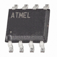
AT93C66-10SI-2.7 Atmel, AT93C66-10SI-2.7 Datasheet

AT93C66-10SI-2.7
Specifications of AT93C66-10SI-2.7
Available stocks
Related parts for AT93C66-10SI-2.7
AT93C66-10SI-2.7 Summary of contents
Page 1
... AT93C46 (1) AT93C56 (2) AT93C66 Note: 1. This device is not recom- mended for new designs. Please refer to AT93C56A. 2. This device is not recom- mended for new designs. Please refer to AT93C66A. ORG GND DO DI VCC DC ORG GND Rev. 0172Y–SEEPR–11/04 1 ...
Page 2
... Meg ohm pullup, then the “x 16” organization is selected. The feature is not available on the 1.8V devices. For the AT93C46, if “x 16” organization is the mode of choice and Pin 6 (ORG) is left unconnected, Atmel recommends using the AT93C46A device. For more details, see the AT93C46A datasheet. Stresses beyond those listed under “Absolute Maximum Ratings” ...
Page 3
Table 2. Pin Capacitance Applicable over recommended operating range from T Symbol Test Conditions C Output Capacitance (DO) OUT C Input Capacitance (CS, SK, DI) IN Note: 1. This parameter is characterized and is not 100% tested. Table 3. ...
Page 4
Table 4. AC Characteristics Applicable over recommended operating range from TTL Gate and 100 pF (unless otherwise noted) Symbol Parameter SK Clock f SK Frequency t SK High Time SKH t SK Low Time SKL Minimum ...
Page 5
... WRITE 1 01 ERAL 1 00 10XXXXXXX WRAL 1 00 01XXXXXXX EWDS 1 00 00XXXXXXX Note: 1. This device is not recommended for new designs. Please refer to AT93C56A. 2. This device is not recommended for new designs. Please refer to AT93C66A. 0172Y–SEEPR–11/04 Address – – 11XXXXX 11XXXX A – – ...
Page 6
... Erase instruction and address are decoded. The DO pin outputs the Ready/Busy status of the part brought high after being kept low for a minimum of 250 ns (t logic “1” at pin DO indicates that the selected memory location has been erased and the part is ready for another instruction. ...
Page 7
... Notes: 1. This device is not recommended for new designs. Please refer to AT93C56A. 2. This device is not recommended for new designs. Please refer to AT93C66A don’t care value, but the extra clock is required don’t care value, but the extra clock is required. 7 0172Y–SEEPR–11/04 µ ...
Page 8
Figure 3. READ Timing High Impedance Figure 4. EWEN Timing Figure 5. EWDS Timing AT93C46/56/66 8 ... ... ...
Page 9
Figure 6. WRITE Timing HIGH IMPEDANCE DO (1) Figure 7. WRAL Timing HIGH IMPEDANCE DO Note: 1. Valid only 4.5V to 5.5V. CC Figure 8. ERASE Timing CS SK ...
Page 10
Figure 9. ERAL Timing HIGH IMPEDANCE DO Note: 1. Valid only 4.5V to 5.5V. CC AT93C46/56/ STANDBY CHECK STATUS BUSY HIGH ...
Page 11
AT93C46 Ordering Information Ordering Code AT93C46-10PI-2.7 AT93C46-10SI-2.7 AT93C46R-10SI-2.7 AT93C46W-10SI-2.7 AT93C46-10TI-2.7 AT93C46-10PI-1.8 AT93C46-10SI-1.8 AT93C46R-10SI-1.8 AT93C46W-10SI-1.8 AT93C46-10TI-1.8 AT93C46-10PU-2.7 AT93C46-10PU-1.8 AT93C46-10SU-2.7 AT93C46-10SU-1.8 AT93C46-10TU-2.7 AT93C46-10TU-1.8 AT93C46Y1-10YU-2.7 AT93C46Y1-10YU-1.8 AT93C46Y5-10YU-2.7 AT93C46Y5-10YU-1.8 AT93C46U3-10UU-2.7 AT93C46U3-10UU-1.8 (2) AT93C46-W2.7-11 (2) AT93C46-W1.8-11 Notes: 1. For 2.7V devices used in the 4.5V ...
Page 12
AT93C56 Ordering Information (2) Ordering Code AT93C56-10PI-2.7 AT93C56-10SI-2.7 AT93C56W-10SI-2.7 AT93C56-10TI-2.7 AT93C56Y1-10YI-2.7 AT93C56-10PI-1.8 AT93C56-10SI-1.8 AT93C56W-10SI-1.8 AT93C56-10TI-1.8 AT93C56Y1-10YI-1.8 Note: 1. This device is not recommended for new designs. Please refer to AT93C56A. 2. For 2.7V devices used in the 4.5V to ...
Page 13
... AT93C66 Ordering Information (2) Ordering Code AT93C66-10PI-2.7 AT93C66-10SI-2.7 AT93C66W-10SI-2.7 AT93C66-10TI-2.7 AT93C66Y1-10YI-2.7 AT93C66-10PI-1.8 AT93C66-10SI-1.8 AT93C66W-10SI-1.8 AT93C66-10TI-1.8 AT93C66Y1-10YI-1.8 Notes: 1. This device is not recommended for new designs. Please refer to AT93C66A. 2. For 2.7V devices used in the 4.5V to 5.5V range, please refer to performance values in Table 3 on page 3 and Table 4 on page 4 ...
Page 14
Packaging Information 8P3 – PDIP Top View PLCS Side View Notes: 1. This drawing is for general information only; refer to JEDEC Drawing MS-001, Variation BA for additional information. 2. Dimensions A and L are measured ...
Page 15
JEDEC SOIC e Side View Note: These drawings are for general information only. Refer to JEDEC Drawing MS-012, Variation AA for proper dimensions, tolerances, datums, etc. 1150 E. Cheyenne Mtn. Blvd. Colorado Springs, CO 80906 R 0172Y–SEEPR–11/04 1 ...
Page 16
EIAJ SOIC 1 N Top View e D Side View Notes: 1. This drawing is for general information only; refer to EIAJ Drawing EDR-7320 for additional information. 2. Mismatch of the upper and lower dies and resin burrs ...
Page 17
TSSOP Pin 1 indicator this corner N Top View Side View Notes: 1. This drawing is for general information only. Refer to JEDEC Drawing MO-153, Variation AA, for proper dimensions, tolerances, datums, ...
Page 18
PIN 1 BALL PAD CORNER Top View PIN 1 BALL PAD CORNER 1 2 (d1 (e1) Bottom View 8 SOLDER BALLS 1. Dimension “b” is measured at the maximum solder ball diameter. This ...
Page 19
MAP D E Top View Side View 2325 Orchard Parkway San Jose, CA 95131 R 0172Y–SEEPR–11/ End View A SYMBOL TITLE 8Y1, 8-lead (4.90 x 3.00 mm ...
Page 20
MAP Pin 1 Index Area D Top View Notes: 1. This drawing is for general information only. Refer to JEDEC Drawing MO-229, for proper dimensions, tolerances, datums, etc. 2. Dimension b applies to metallized terminal and is measured ...
Page 21
... Disclaimer: The information in this document is provided in connection with Atmel products. No license, express or implied, by estoppel or otherwise, to any intellectual property right is granted by this document or in connection with the sale of Atmel products. EXCEPT AS SET FORTH IN ATMEL’S TERMS AND CONDI- TIONS OF SALE LOCATED ON ATMEL’S WEB SITE, ATMEL ASSUMES NO LIABILITY WHATSOEVER AND DISCLAIMS ANY EXPRESS, IMPLIED OR STATUTORY WARRANTY RELATING TO ITS PRODUCTS INCLUDING, BUT NOT LIMITED TO, THE IMPLIED WARRANTY OF MERCHANTABILITY, FITNESS FOR A PARTICULAR PURPOSE, OR NON-INFRINGEMENT ...


