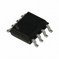
FM93C86AM8 Fairchild Semiconductor, FM93C86AM8 Datasheet

FM93C86AM8
Specifications of FM93C86AM8
Available stocks
Related parts for FM93C86AM8
FM93C86AM8 Summary of contents
Page 1
... SO and DIP packages INSTRUCTION DI REGISTER ADDRESS REGISTER ORG DECODER DO © 2000 Fairchild Semiconductor International FM93C86A Rev. C.1 I Wide V 2. User selectable organization x16 (ORG = 1) x8 (ORG = 0) I Typical active current of 200µA 10µA standby current typical 1µA standby current typical (L) ...
Page 2
Pins designated as "NC" are typically unbonded pins. However some of them are bonded for special testing purposes. Hence if a signal is applied to these pins, care should be taken that the voltage applied on these pins does not ...
Page 3
Ambient Storage Temperature All Input or Output Voltages with Respect to Ground Lead Temperature (Soldering, 10 sec.) ESD rating I Operating Current CCA I Standby Current CCS I Input Leakage IL I Output Leakage OL I Input Leakage ORG Pin ...
Page 4
Ambient Storage Temperature All Input or Output Voltages with Respect to Ground Lead Temperature (Soldering, 10 sec.) ESD rating page 3 for 4. Operating Current CCA I Standby Current CCS L LZ (2.7V to 4.5V) ...
Page 5
... A typical communication on the Microwire bus is made through the CS, SK, DI and DO signals. To facilitate various operations on the Memory array, a set of 7 instructions are implemented on FM93C86A. The format of each instruction is listed under Table 1 (for 16-bit format) and Table 2 (for 8-bit format). ...
Page 6
... X X WRITE instruction allows write operation to a specified location in the memory with a specified data. This instruction is valid only when device is write-enabled (Refer WEN instruction). Input information (Start bit, Opcode, Address and Data) for this WRITE instruction should be issued as listed under Table 1 or Table 2 ...
Page 7
Write Disable (WDS) instruction disables all programming opera- tions and should follow all programming operations. Executing this instruction after a valid write instruction would protect against accidental data disturb due to spurious noise, glitches, inadvert- ent writes etc. Input information ...
Page 8
SYNCHRONOUS DATA TIMING CS t CSS SK t DIS Valid Input DI DO (Data Read (Status Read) READ CYCLE (READ ...
Page 9
WRITE DISABLE CYCLE (WDS = ...
Page 10
ERASE CYCLE (ERASE Star t Bit DO A 93C86A (ORG=1; n Address bits patter n -> A9-A8-A7-A6-A5-A4-A3-A2-A1-A0; User defined A 93C86A (ORG=0; n Address bits patter n -> A10-A9-A8-A7-A6-A5-A4-A3-A2-A1-A0; User defined ERASE ALL CYCLE (ERAL) CS ...
Page 11
All lead tips Typ. All Leads FM93C86A Rev. C.1 0.189 - 0.197 (4.800 ...
Page 12
... Fairchild's products are not authorized for use as critical components in life support devices or systems without the express written approval of the President of Fairchild Semiconductor Corporation. As used herein: 1. Life support devices or systems are devices or systems which, (a) are intended for surgical implant into the body, or (b) support ...


