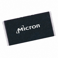
MT28F004B3VG-8 BET TR Micron Technology Inc, MT28F004B3VG-8 BET TR Datasheet - Page 9

MT28F004B3VG-8 BET TR
Manufacturer Part Number
MT28F004B3VG-8 BET TR
Description
IC FLASH 4MBIT 80NS 40TSOP
Manufacturer
Micron Technology Inc
Datasheet
1.MT28F004B3VG-8_B.pdf
(30 pages)
Specifications of MT28F004B3VG-8 BET TR
Format - Memory
FLASH
Memory Type
FLASH - Nor
Memory Size
4M (512K x 8)
Speed
80ns
Interface
Parallel
Voltage - Supply
3 V ~ 3.6 V
Operating Temperature
-40°C ~ 85°C
Package / Case
40-TSOP
Lead Free Status / RoHS Status
Contains lead / RoHS non-compliant
Parameter Blocks
and more frequently changing system parameters and
also may store configuration or diagnostic coding.
These blocks are enabled for erasure when the V
is at V
required.
Main Memory Blocks
memory blocks and do not require a super-voltage on
RP# or WP# control to be erased or written. These
blocks are intended for code storage, ROM-resident
applications or operating systems that require in-sys-
tem update capability.
Output (READ) Operations
different types of READs. Depending on the current
mode of the device, a READ operation produces data
from the memory array, status register or device iden-
tification register. In each of these three cases, the
WE#, CE# and OE# inputs are controlled in a similar
manner. Moving between modes to perform a specific
READ is described in the Command Execution section.
Memory Array
OE# and CE# must be LOW. Valid data is output on the
DQ pins when these conditions have been met and a
valid address is given. Valid data remains on the DQ
pins until the address changes, or until OE# or CE#
goes HIGH, whichever occurs first. The DQ pins con-
tinue to output new data after each address transition
as long as OE# and CE# remain LOW.
When the memory array is accessed as a 256K x 16,
BYTE# is HIGH, and data is output on DQ0–DQ15. To
access the memory array as a 512K x 8, BYTE# must be
LOW, DQ8–DQ14 must be High-Z, and all data must be
output on DQ0–DQ7. The DQ15/A-1 pin becomes the
lowest order address input so that 524,288 locations
can be read.
cally in the array read mode. All commands and their
operations are described in the Command Set and
Command Execution sections.
09005aef8114a789
F45.fm - Rev. E 6/04 EN
The two 8KB parameter blocks store less sensitive
The four remaining blocks are general-purpose
The MT28F004B3 and MT28F400B3 feature three
To read the memory array, WE# must be HIGH, and
The MT28F400B3 features selectable bus widths.
After power-up or RESET, the device is automati-
PPH
. No super-voltage unlock or WP# control is
PP
SMART 3 BOOT BLOCK FLASH MEMORY
pin
9
Status Register
the same input sequencing as a READ of the array
except that the address inputs are “Don’t Care.” The
status register contents are always output on DQ0–
DQ7, regardless of the condition of BYTE# on the
MT28F400B3. DQ8–DQ15 are LOW when BYTE# is
HIGH, and DQ8–DQ14 are High-Z when BYTE# is
LOW. Data from the status register is latched on the
falling edge of OE# or CE#, whichever occurs last. If the
contents of the status register change during a READ of
the status register, either OE# or CE# may be toggled
while the other is held LOW to update the output.
cally enters the status register read mode. In addition,
a READ during a WRITE or ERASE produces the status
register contents on DQ0–DQ7. When the device is in
the erase suspend mode, a READ operation produces
the status register contents until another command is
issued. In certain other modes, READ STATUS REGIS-
TER may be given to return to the status register read
mode. All commands and their operations are
described in the Command Set and Command Execu-
tion sections.
Identification Register
ters requires the same input sequencing as a READ of
the array. WE# must be HIGH, and OE# and CE# must
be LOW. However, ID register data is output only on
DQ0–DQ7, regardless of the condition of BYTE# on the
MT28F400B3. A0 is used to decode between the two
bytes of the device ID register; all other address inputs
are “Don’t Care.” When A0 is LOW, the manufacturer
compatibility ID is output, and when A0 is HIGH, the
device ID is output. DQ8–DQ15 are High-Z when
BYTE# is LOW. When BYTE# is HIGH, DQ8–DQ15 are
00h when the manufacturer compatibility ID is read
and 44h when the device ID is read.
READ IDENTIFICATION may be issued while the
device is in certain other modes. In addition, the iden-
tification register read mode can be reached by apply-
ing a super-voltage (V
method, the ID register can be read while the device is
in any mode. When A9 is returned to V
device returns to the previous mode.
Performing a READ of the status register requires
Following a WRITE or ERASE, the device automati-
A READ of the two 8-bit device identification regis-
To get to the identification register read mode,
Micron Technology, Inc., reserves the right to change products or specifications without notice.
ID
) to the A9 pin. Using this
©2003 Micron Technology, Inc. All rights reserved.
IL
or V
4Mb
IH
, the


