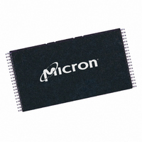
MT28F004B3VG-8 TET TR Micron Technology Inc, MT28F004B3VG-8 TET TR Datasheet - Page 7

MT28F004B3VG-8 TET TR
Manufacturer Part Number
MT28F004B3VG-8 TET TR
Description
IC FLASH 4MBIT 80NS 40TSOP
Manufacturer
Micron Technology Inc
Datasheet
1.MT28F004B3VG-8_B.pdf
(30 pages)
Specifications of MT28F004B3VG-8 TET TR
Format - Memory
FLASH
Memory Type
FLASH - Nor
Memory Size
4M (512K x 8)
Speed
80ns
Interface
Parallel
Voltage - Supply
3 V ~ 3.6 V
Operating Temperature
-40°C ~ 85°C
Package / Case
40-TSOP
Lead Free Status / RoHS Status
Contains lead / RoHS non-compliant
Functional Description
incorporate a number of features ideally suited for sys-
tem firmware. The memory array is segmented into
individual erase blocks. Each block may be erased
without affecting data stored in other blocks. These
memory blocks are read, written and erased with com-
mands to the command execution logic (CEL). The
CEL controls the operation of the internal state
machine (ISM), which completely controls all WRITE,
BLOCK ERASE and VERIFY operations. The ISM pro-
tects each memory location from over-erasure and
optimizes each memory location for maximum data
retention. In addition, the ISM greatly simplifies the
control necessary for writing the device insystem or in
an external programmer.
mation on the operation of the MT28F004B3 and
MT28F400B3 and is organized into these sections:
Overview
Smart 3 Technology (B3)
insystem READ, WRITE and ERASE operations. WRITE
and ERASE operations may be executed with a V
voltage of 3.3V or 5V. Due to process technology
advances, 5V V
duction programming.
Seven Independently Erasable Memory
Blocks
into seven independently erasable memory blocks that
allow portions of the memory to be erased without
affecting the rest of the memory data. A special boot
block is hardware-protected against inadvertent era-
sure or writing by requiring either a super-voltage on
the RP# pin or driving the WP# pin HIGH. One of these
two conditions must exist along with the V
09005aef8114a789
F45.fm - Rev. E 6/04 EN
The MT28F004B3 and MT28F400B3 Flash devices
The Functional Description provides detailed infor-
• Overview
• Memory Architecture
• Output (READ) Operations
• Input Operations
• Command Set
• ISM Status Register
• Command Execution
• Error Handling
• WRITE/ERASE Cycle Endurance
• Power Usage
• Power-Up
Smart 3 technology allows maximum flexibility for
The MT28F004B3 and MT28F400B3 are organized
PP
is optimal for application and pro-
PP
voltage
SMART 3 BOOT BLOCK FLASH MEMORY
PP
7
(3.3V or 5V) on the V
performed on the boot block. The remaining blocks
require only the V
before writing or erasing.
Hardware-Protected Boot block
written only when the RP# pin is taken to V
the WP# pin is brought HIGH. This provides additional
security for the core firmware during in-system firm-
ware updates should an unintentional power fluctua-
tion or system reset occur. The MT28F004B3 and
MT28F400B3 are available with the boot block starting
at the bottom of the address space (“B” suffix) or the
top of the address space (“T” suffix).
Selectable Bus Size (MT28F400B3 ONLY)
x 8) or 16-bit (256K x 16) data bus for reading and writ-
ing the memory. The BYTE# pin is used to select the
bus width. In the x16 configuration, control data is
read or written only on the lower eight bits (DQ0–
DQ7).
data pins for the selected configuration. When the x8
configuration is selected, data is written in byte form;
when the x16 configuration is selected, data is written
in word form.
Internal State Machine (ISM)
simplified with an ISM that controls all erase and write
algorithms in the memory array. The ISM ensures pro-
tection against overerasure and optimizes write mar-
gin to each cell.
increments and monitors WRITE attempts, verifies
write margin on each memory cell and updates the
ISM status register. When BLOCK ERASE is performed,
the ISM automatically overwrites the entire addressed
block (eliminates overerasure), increments and moni-
tors ERASE attempts, and sets bits in the ISM status
register.
ISM Status Register
sor to monitor the status of the ISM during WRITE and
ERASE operations. Two bits of the 8-bit status register
are set and cleared entirely by the ISM. These bits indi-
cate whether the ISM is busy with a WRITE or ERASE
This block of the memory array can be erased or
The MT28F400B3 allows selection of an 8-bit (512K
Data written to the memory array utilizes all active
BLOCK ERASE and BYTE/WORD WRITE timing are
During WRITE operations, the ISM automatically
The ISM status register enables an external proces-
Micron Technology, Inc., reserves the right to change products or specifications without notice.
PP
PP
voltage be present on the V
pin before a WRITE or ERASE is
©2003 Micron Technology, Inc. All rights reserved.
HH
4Mb
or when
PP
pin


