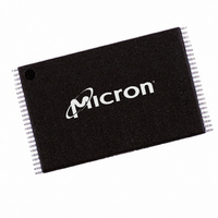
MT29F8G08FACWP:C TR Micron Technology Inc, MT29F8G08FACWP:C TR Datasheet - Page 26

MT29F8G08FACWP:C TR
Manufacturer Part Number
MT29F8G08FACWP:C TR
Description
IC FLASH 8GBIT 48TSOP
Manufacturer
Micron Technology Inc
Datasheet
1.MT29F2G08AACWPC_TR.pdf
(58 pages)
Specifications of MT29F8G08FACWP:C TR
Format - Memory
FLASH
Memory Type
FLASH - Nand
Memory Size
8G (1G x 8)
Interface
Parallel
Voltage - Supply
2.7 V ~ 3.6 V
Operating Temperature
0°C ~ 70°C
Package / Case
48-TSOP
Lead Free Status / RoHS Status
Lead free / RoHS Compliant
Speed
-
READ STATUS 70h
Table 11:
Figure 18:
PDF: 09005aef814b01a2 / Source: 09005aef814b01c7
2_4_8gb_nand_m49a__2.fm - Rev. D 12/06 EN
[15:8]
Bit
SR
0
1
2
3
4
5
6
7
WE#
Write protect
I/Ox
CE#
RE#
CLE
Ready/busy
Ready/busy
Program
Pass/fail
Page
Status Register Bit Definition
–
–
–
–
–
Status Register Operation
Notes: 1. Status register bit 5 is “0” during the actual programming operation. If cache mode is
Program Page
Cache Mode
Pass/fail (N-1)
Write protect
Ready/busy
Pass/fail (N)
Ready/busy
cache
NAND Flash devices have an 8-bit status register that the software can read during
device operation. On the x16 device, I/O[15:8] are “0” when the status register is being
read. Table 11 describes the status register.
After a READ STATUS command, all READ cycles will be from the status register until a
new command is issued. Changes in the status register will be seen on I/O[7:0] as long
as CE# and RE# are LOW; it is not necessary to start a new READ STATUS cycle to see
these changes.
While monitoring the read status to determine when the
array to data register) is complete, the user must re-issue the READ (00h) command to
make the change from status mode to read mode. After the READ command has been
re-issued, pulsing the RE# line will result in outputting data, starting from the initial col-
umn address.
2. Status register bit 6 is “1” when the cache is ready to accept new data. R/B# follows bit 6.
–
–
–
–
used, this bit will be “1” when all internal operations are complete.
See Figure 16 on page 23 and Figure 21 on page 28.
2
1
70h
Write protect Write protect
Page Read
Ready/busy
Ready/busy
–
–
–
–
–
–
t CLR
Cache Mode
Ready/busy
Page Read
Ready/busy
cache
26
2Gb, 4Gb, 8Gb: x8, x16 NAND Flash Memory
–
–
–
–
–
–
2
1
Micron Technology, Inc., reserves the right to change products or specifications without notice.
t REA
Write protect “0” = Protected
Block Erase
Ready/busy
Ready/busy
Pass/fail
–
–
–
–
–
Status output
“0” = Successful PROGRAM/ERASE
“1” = Error in PROGRAM/ERASE
“0” = Successful PROGRAM/ERASE
“1” = Error in PROGRAM/ERASE
“0”
“0”
“0”
“0” = Busy
“1” = Ready
“0” = Busy
“1” = Ready
“1” = Not protected
“0”
t
R (transfer from NAND Flash
Command Definitions
©2005 Micron Technology, Inc. All rights reserved.
Definition


