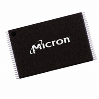
MT29F8G08FACWP:C TR Micron Technology Inc, MT29F8G08FACWP:C TR Datasheet - Page 32

MT29F8G08FACWP:C TR
Manufacturer Part Number
MT29F8G08FACWP:C TR
Description
IC FLASH 8GBIT 48TSOP
Manufacturer
Micron Technology Inc
Datasheet
1.MT29F2G08AACWPC_TR.pdf
(58 pages)
Specifications of MT29F8G08FACWP:C TR
Format - Memory
FLASH
Memory Type
FLASH - Nand
Memory Size
8G (1G x 8)
Interface
Parallel
Voltage - Supply
2.7 V ~ 3.6 V
Operating Temperature
0°C ~ 70°C
Package / Case
48-TSOP
Lead Free Status / RoHS Status
Lead free / RoHS Compliant
Speed
-
One-Time Programmable (OTP) Area
OTP DATA PROGRAM A0h-10h
PDF: 09005aef814b01a2 / Source: 09005aef814b01c7
2_4_8gb_nand_m49a__2.fm - Rev. D 12/06 EN
This Micron NAND Flash device offers a protected, one-time programmable NAND
Flash memory area. Ten full pages (2,112 bytes or 1,056 words per page) of OTP data is
available on the device, and the entire range is guaranteed to be good from the factory.
The OTP area is accessible only through the OTP commands. Customers can use the
OTP area any way they desire; typical uses include programming serial numbers or
other data for permanent storage.
In Micron NAND Flash devices, the OTP area leaves the factory in a non-written state
(all bits are “1s”). Programming or partial-page programming enables the user to pro-
gram only “0” bits in the OTP area. The OTP area cannot be erased, even if it is not pro-
tected. Protecting the OTP area simply prevents further programming of the OTP area.
While the OTP area is referred to as “one-time programmable,” Micron provides a
unique way to program and verify data—before permanently protecting it and prevent-
ing future changes.
OTP programming and protection are accomplished in two discrete operations. First,
using the OTP DATA PROGRAM (A0h-10h) command, an OTP page is programmed
entirely in one operation, or in up to four partial-page programming sequences. Second,
the OTP area is permanently protected from further programming using the OTP DATA
PROTECT (A5h-10h) command. The pages within the OTP area can always be read using
the OTP DATA READ (AFh-30h) command, whether or not it is protected.
The OTP DATA PROGRAM (A0h-10h) command is used to write data to the pages within
the OTP area. An entire page can be programmed at one time, or the page can be par-
tially programmed up to four times. There is no ERASE operation for the OTP pages.
The OTP DATA PROGRAM enables programming into an offset of an OTP page, using
the two bytes of column address (CA[11:0]). The command is not compatible with the
RANDOM DATA INPUT (85h) command. The OTP DATA PROGRAM command will not
execute if the OTP area has been protected.
To use the OTP DATA PROGRAM command, issue the A0h command. Then issue 5
ADDRESS cycles: the first 2 ADDRESS cycles are the column address, and for the
remaining 3 cycles, select a page in the range of 02h-00h-00h through 0Bh-00h-00h.
Next, write the data: from 1 to 2,112 bytes (x8 device), or from 1 to 1,056 words (x16
device). After data input is complete, issue the 10h command. The internal control logic
automatically executes the proper programming algorithm and controls the necessary
timing for programming and verification. Program verification only detects “1s” that are
not successfully written to “0s.”
R/B# goes LOW during the duration of the array programming time (
STATUS (70h) command is the only command valid during the OTP DATA PROGRAM
operation. Bit 5 of the status register will reflect the state of R/B#. If bit 7 is “0,” the OTP
area has been protected; otherwise, it is not protected.
When the device is ready, read bit 0 of the status register to determine if the operation
passed or failed (see Table 11 on page 26).
It is possible to program each OTP page a maximum of four times.
32
2Gb, 4Gb, 8Gb: x8, x16 NAND Flash Memory
Micron Technology, Inc., reserves the right to change products or specifications without notice.
Command Definitions
©2005 Micron Technology, Inc. All rights reserved.
t
PROG). The READ


