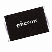
MT29F8G08FACWP:C TR Micron Technology Inc, MT29F8G08FACWP:C TR Datasheet - Page 6

MT29F8G08FACWP:C TR
Manufacturer Part Number
MT29F8G08FACWP:C TR
Description
IC FLASH 8GBIT 48TSOP
Manufacturer
Micron Technology Inc
Datasheet
1.MT29F2G08AACWPC_TR.pdf
(58 pages)
Specifications of MT29F8G08FACWP:C TR
Format - Memory
FLASH
Memory Type
FLASH - Nand
Memory Size
8G (1G x 8)
Interface
Parallel
Voltage - Supply
2.7 V ~ 3.6 V
Operating Temperature
0°C ~ 70°C
Package / Case
48-TSOP
Lead Free Status / RoHS Status
Lead free / RoHS Compliant
Speed
-
General Description
Figure 3:
PDF: 09005aef814b01a2 / Source: 09005aef814b01c7
2_4_8gb_nand_m49a__2.fm - Rev. D 12/06 EN
NAND Flash Functional Block Diagram
NAND Flash technology provides a cost-effective solution for applications requiring
high-density, solid-state storage. Micron MT29F2G08AxC and MT29F2G16AxC devices
are 2Gb NAND Flash memory devices. The MT29F4G08BxC and MT29F4G16BxC are
4Gb devices. The MT29F8G08FAC is a four-die stack that operates as two independent
4Gb devices, providing a total storage capacity of 8Gb in a single, space-saving package.
These devices include standard NAND Flash features as well as new features designed to
enhance system-level performance.
Micron NAND Flash devices use a highly multiplexed 8- or 16-bit bus (I/O[7:0] or
I/O[15:0]) to transfer data, addresses, and instructions. The five command pins (CLE,
ALE, CE#, RE#, WE#) implement the NAND Flash command bus interface protocol. Two
additional pins control hardware write protection (WP#) and monitor device status
(R/B#).
This hardware interface creates a low-pin-count device with a standard pinout that is
the same from one density to another, supporting future upgrades to higher densities
without board redesign.
The MT29F2G and MT29F4G devices contain 2,048 and 4,096 erasable blocks, respec-
tively. Each block is subdivided into 64 programmable pages. Each page consists of
2,112 bytes (x8) or 1,056 words (x16). The pages are further divided into a 2,048-byte data
storage region with a separate 64-byte area on the x8 device; and on the x16 device, sep-
arate 1,024-word and 32-word areas. The 64-byte and 32-word areas are typically used
for error management functions.
The contents of each 2,112-byte page can be programmed in 300µs, and an entire 132K-
byte/66K-word block can be erased in 2ms. On-chip control logic automates PROGRAM
and ERASE operations to maximize cycle endurance. ERASE/PROGRAM endurance is
specified at 100,000 cycles when appropriate error correction code (ECC) and error
management are used.
I/O [7:0]
I/O [15:0]
R/B#
WE#
WP#
ALE
CE#
CLE
RE#
Control
Control
Logic
I/O
Command Register
Address Register
Status Register
6
2Gb, 4Gb, 8Gb: x8, x16 NAND Flash Memory
Micron Technology, Inc., reserves the right to change products or specifications without notice.
General Description
©2005 Micron Technology, Inc. All rights reserved.
Column Decode
Cache Register
Data Register
V
CC
V
SS


