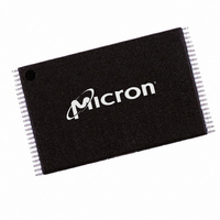
MT29F8G08FACWP:C TR Micron Technology Inc, MT29F8G08FACWP:C TR Datasheet - Page 8

MT29F8G08FACWP:C TR
Manufacturer Part Number
MT29F8G08FACWP:C TR
Description
IC FLASH 8GBIT 48TSOP
Manufacturer
Micron Technology Inc
Datasheet
1.MT29F2G08AACWPC_TR.pdf
(58 pages)
Specifications of MT29F8G08FACWP:C TR
Format - Memory
FLASH
Memory Type
FLASH - Nand
Memory Size
8G (1G x 8)
Interface
Parallel
Voltage - Supply
2.7 V ~ 3.6 V
Operating Temperature
0°C ~ 70°C
Package / Case
48-TSOP
Lead Free Status / RoHS Status
Lead free / RoHS Compliant
Speed
-
Table 1:
PDF: 09005aef814b01a2 / Source: 09005aef814b01c7
2_4_8gb_nand_m49a__2.fm - Rev. D 12/06 EN
MT29FxG08
MT29FxG16
R/B#, R/B2#
CE#, CE2#
I/O[15:0]
Symbol
I/O[7:0]
DNU
WE#
WP#
ALE
CLE
RE#
V
V
NC
CC
SS
Pin Descriptions
Output
Supply
Supply
Input
Input
Input
Input
Input
Input
Type
I/O
–
–
Address latch enable: During the time ALE is HIGH, address information is
transferred from I/O[7:0] into the on-chip address register upon a LOW-to-HIGH
transition on WE#
should be driven LOW.
Chip enable: This gates transfers between the host system and the NAND Flash
device. Once the device starts a PROGRAM or ERASE operation, the chip enable
pin can be de-asserted.
For the 8Gb configuration, CE# controls the first 4Gb of memory; CE2# controls
the second 4Gb. See “Bus Operation” on page 16 for additional operational
details.
In the 8Gb configuration, R/B# is for the 4Gb of memory enabled by CE#; R/B2# is
for the 4Gb of memory enabled by the CE2#.
Command latch enable: When CLE is HIGH, information is transferred from
I/O[7:0] to the on-chip command register on the rising edge of WE#. When
command information is not being loaded, CLE should be driven LOW.
Read enable: This gates transfers from the NAND Flash device to the host system.
Write enable: This gates transfers from the host system to the NAND Flash device.
Write protect: Pin protects against inadvertent PROGRAM and ERASE operations.
All PROGRAM and ERASE operations are disabled when the WP# pin is LOW.
Data inputs/outputs: The bidirectional I/O pins transfer address, data, and
instruction information. Data is output only during READ operations; at other
times the I/O pins are inputs.
Ready/busy: An open-drain, active-LOW output that uses an external pull-up
resistor, the pin is used to indicate when the chip is processing a PROGRAM or
ERASE operation. The pin is also used during a READ operation to indicate when
data is being transferred from the array into the serial data register. When these
operations have completed, the R/B# returns to the High-Z state.
V
V
No connect: NC pins are not internally connected. These pins can be driven or left
unconnected.
Do not use: These pins must be left unconnected.
CC
SS
: Ground connection.
: Power supply.
.
When address information is not being loaded, the ALE pin
8
2Gb, 4Gb, 8Gb: x8, x16 NAND Flash Memory
Micron Technology, Inc., reserves the right to change products or specifications without notice.
Description
Pin Assignments and Descriptions
©2005 Micron Technology, Inc. All rights reserved.


