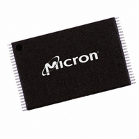
MT29F8G08BAAWP:A TR Micron Technology Inc, MT29F8G08BAAWP:A TR Datasheet - Page 15

MT29F8G08BAAWP:A TR
Manufacturer Part Number
MT29F8G08BAAWP:A TR
Description
IC FLASH 8GBIT 48TSOP
Manufacturer
Micron Technology Inc
Datasheet
1.MT29F16G08DAAWP-ETA_TR.pdf
(81 pages)
Specifications of MT29F8G08BAAWP:A TR
Format - Memory
FLASH
Memory Type
FLASH - Nand
Memory Size
8G (1G x 8)
Interface
Parallel
Voltage - Supply
2.7 V ~ 3.6 V
Operating Temperature
0°C ~ 70°C
Package / Case
48-TSOP
Lead Free Status / RoHS Status
Lead free / RoHS Compliant
Speed
-
Bus Operation
Control Signals
Commands
Address Input
PDF: 09005aef81b80e13/Source: 09005aef81b80eac
4gb_nand_m40a__2.fm - Rev. B 2/07 EN
The bus on MT29Fxxx devices is multiplexed. Data I/O, addresses, and commands all
share the same pins, I/O[7:0].
The command sequence normally consists of a COMMAND LATCH cycle, ADDRESS
INPUT cycles, and 1 or more DATA cycles—either READ or WRITE.
CE#, WE#, RE#, CLE, ALE, and WP# control NAND Flash device READ and WRITE opera-
tions. On the 8Gb MT29F8G08DAA, CE# and CE2# each control independent 4Gb arrays.
On the 16Gb MT29F16G08FAA, CE# and CE2# each control independent 8Gb arrays.
CE2# functions the same as CE# for its own array; all operations described for CE# also
apply to CE2#.
CE# is used to enable the device. When CE# is LOW and the device is not in the busy
state, the NAND Flash memory will accept command, address, and data information.
When the device is not performing an operation, the CE# pin is typically driven HIGH
and the device enters standby mode. The memory will enter standby if CE# goes HIGH
while data is being transferred and the device is not busy. This helps reduce power
consumption. See Figure 61 on page 69 and Figure 69 on page 75 for examples of CE#
“Don’t Care” operations.
The CE# “Don’t Care” operation enables the NAND Flash to reside on the same asyn-
chronous memory bus as other Flash or SRAM devices. Other devices on the memory
bus can then be accessed while the NAND Flash is busy with internal operations. This
capability is important for designs that require multiple NAND Flash devices on the
same bus.
A HIGH CLE signal indicates that a command cycle is taking place. A HIGH ALE signal
signifies that an ADDRESS INPUT cycle is occurring.
Commands are written to the command register on the rising edge of WE# when:
• CE# and ALE are LOW, and
• CLE is HIGH, and
• The device is not busy
As exceptions, the device accepts the READ STATUS, TWO-PLANE/MULTIPLE-DIE
READ STATUS, and RESET commands when busy. Commands are transferred to the
command register on the rising edge of WE# (see Figure 53 on page 65). Commands are
input on I/O[7:0].
Addresses are written to the address register on the rising edge of WE# when:
• CE# and CLE are LOW, and
• ALE is HIGH
Addresses are input on I/O[7:0]. Bits not part of the address space must be LOW.
The number of ADDRESS cycles required for each command varies. Refer to the
command descriptions to determine addressing requirements (see Table 6 on page 19).
15
4Gb, 8Gb, and 16Gb x8 NAND Flash Memory
Micron Technology, Inc., reserves the right to change products or specifications without notice.
©2006 Micron Technology, Inc. All rights reserved.
Bus Operation


