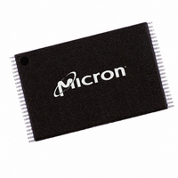
MT29F8G08BAAWP:A TR Micron Technology Inc, MT29F8G08BAAWP:A TR Datasheet - Page 30

MT29F8G08BAAWP:A TR
Manufacturer Part Number
MT29F8G08BAAWP:A TR
Description
IC FLASH 8GBIT 48TSOP
Manufacturer
Micron Technology Inc
Datasheet
1.MT29F16G08DAAWP-ETA_TR.pdf
(81 pages)
Specifications of MT29F8G08BAAWP:A TR
Format - Memory
FLASH
Memory Type
FLASH - Nand
Memory Size
8G (1G x 8)
Interface
Parallel
Voltage - Supply
2.7 V ~ 3.6 V
Operating Temperature
0°C ~ 70°C
Package / Case
48-TSOP
Lead Free Status / RoHS Status
Lead free / RoHS Compliant
Speed
-
Figure 20:
Figure 21:
BLOCK ERASE Operation
BLOCK ERASE 60h-D0h
PDF: 09005aef81b80e13/Source: 09005aef81b80eac
4gb_nand_m40a__2.fm - Rev. B 2/07 EN
INTERNAL DATA MOVE Operation
INTERNAL DATA MOVE Operation with RANDOM DATA INPUT
Notes:
STATUS command can be used instead of the R/B# line to determine when the write is
complete. When status register bit 6 = 1, bit 0 of the status register indicates if the opera-
tion was successful.
The RANDOM DATA INPUT (85h) command can be used during the PROGRAM for
INTERNAL DATA MOVE command sequence to modify one or more bytes of the orig-
inal data. First, data is copied into the cache register using the 00h-35h command
sequence, then the RANDOM DATA INPUT (85h) command is written along with the
address of the data to be modified next. New data is input on the external data pins. This
copies the new data into the cache register.
When 10h is written to the command register, the original data plus the modified data
are transferred to the data register, and programming of the new page is started. The
RANDOM DATA INPUT command can be issued as many times as necessary before
starting the programming sequence with 10h (see Figures 20 and 21).
Because INTERNAL DATA MOVE operations do not use external memory, ECC cannot
be used to check for errors before programming the data to a new page. This can lead to
a data error if the source page contains a bit error due to charge loss or charge gain. In
the case that multiple INTERNAL DATA MOVE operations are performed, these bit
errors may accumulate without correction. For this reason, it is highly recommended
that systems using INTERNAL DATA MOVE operations also use a robust ECC scheme
that can correct two or more bits per sector.
R/B#
1. INTERNAL DATA MOVE operations are only supported within the plane from which data is
R/B#
Erasing occurs at the block level. For example, the MT29F4G08AAA device has 4,096
erase blocks, organized into 64 pages per block, 2,112 bytes per page (2,048 + 64 bytes).
Each block is 132K bytes (128K + 4K bytes). The BLOCK ERASE command operates on
one block at a time (see Figure 22 on page 31).
Three cycles of addresses BA[18:6] and PA[5:0] are required. Although page addresses
PA[5:0] are loaded, they are a “Don’t Care” and are ignored for BLOCK ERASE opera-
tions. See Table 3 on page 13 for addressing details.
I/Ox
I/Ox
read.
00h
00h
(5 cycles)
Address
(5 cycles)
Address
35h
35h
t R
85h
t R
30
4Gb, 8Gb, and 16Gb x8 NAND Flash Memory
(5 cycles)
Address
85h
Micron Technology, Inc., reserves the right to change products or specifications without notice.
(5 cycles)
Address
Data
85h
Unlimited number
of repetitions
10h
(2 cycles)
Address
t PROG
Data
Command Definitions
©2006 Micron Technology, Inc. All rights reserved.
10h
70h
t PROG
70h
Status
Status


