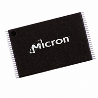
MT29F8G08BAAWP:A TR Micron Technology Inc, MT29F8G08BAAWP:A TR Datasheet - Page 58

MT29F8G08BAAWP:A TR
Manufacturer Part Number
MT29F8G08BAAWP:A TR
Description
IC FLASH 8GBIT 48TSOP
Manufacturer
Micron Technology Inc
Datasheet
1.MT29F16G08DAAWP-ETA_TR.pdf
(81 pages)
Specifications of MT29F8G08BAAWP:A TR
Format - Memory
FLASH
Memory Type
FLASH - Nand
Memory Size
8G (1G x 8)
Interface
Parallel
Voltage - Supply
2.7 V ~ 3.6 V
Operating Temperature
0°C ~ 70°C
Package / Case
48-TSOP
Lead Free Status / RoHS Status
Lead free / RoHS Compliant
Speed
-
Figure 51:
Error Management
PDF: 09005aef81b80e13/Source: 09005aef81b80eac
4gb_nand_m40a__2.fm - Rev. B 2/07 EN
PROGRAM Disable
WE#
WP#
This NAND Flash device is specified to have a minimum of 4,016 valid blocks (N
of every 4,096 total available blocks. This means the devices may have blocks that are
invalid when shipped from the factory. An invalid block is one that contains one or more
bad bits. Additional bad blocks may develop with use. However, the total number of
available blocks will not fall below N
Although NAND Flash memory devices may contain bad blocks, they can be used quite
reliably in systems that provide bad-block management and error correction algo-
rithms. This type of software environment ensures data integrity.
Internal circuitry isolates each block from other blocks, so the presence of a bad block
does not affect the operation of the rest of the NAND Flash array.
The first block (physical block address 00h) for each CE# is guaranteed to be valid with
ECC (up to 1,000 PROGRAM/ERASE cycles) when shipped from the factory. This
provides a reliable location for storing boot code and critical boot information.
NAND Flash devices are shipped from the factory erased. The factory identifies invalid
blocks before shipping by programming data other than FFh into the first spare location
(column address 2,048) of the first or second page of each bad block.
System software should check the first spare address on the first and second page of
each block prior to performing any PROGRAM or ERASE operations on the NAND Flash
device. A bad-block table can then be created, allowing system software to map around
these areas. Factory testing is performed under worst-case conditions. Because blocks
marked “bad” may be marginal, it may not be possible to recover this information if the
block is erased.
Over time, some memory locations may fail to program or erase properly. In order to
ensure that data is stored properly over the life of the NAND Flash device, the following
precautions are required:
• Check status after a PROGRAM, ERASE, or INTERNAL DATA MOVE operation.
• Under typical use conditions, utilize a minimum of 1-bit ECC per 528 bytes of data.
• Use bad-block management and a wear-leveling algorithm.
R/B#
I/Ox
t WW
80h
58
4Gb, 8Gb, and 16Gb x8 NAND Flash Memory
VB
10h
Micron Technology, Inc., reserves the right to change products or specifications without notice.
during the endurance life of the product.
©2006 Micron Technology, Inc. All rights reserved.
Error Management
VB
) out


