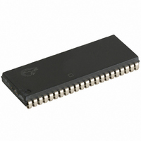
CY7C1041B-15VC Cypress Semiconductor Corp, CY7C1041B-15VC Datasheet

CY7C1041B-15VC
Specifications of CY7C1041B-15VC
Related parts for CY7C1041B-15VC
CY7C1041B-15VC Summary of contents
Page 1
... TTL-compatible inputs and outputs • Easy memory expansion with CE and OE features Functional Description The CY7C1041B is a high-performance CMOS static RAM or- ganized as 262,144 words by 16 bits. Writing to the device is accomplished by taking Chip Enable (CE) and Write Enable (WE) inputs LOW. If Byte Low Enable ...
Page 2
... Com’ 1/t MAX RC Ind’ > > < MAX , Com’l CC – 0.3V, CC Com’l L > V – 0.3V < 0.3V Ind’ CY7C1041B [1] –0. 0.5V CC Ambient [2] Temperature + – +85 C 7C1041B-15 7C1041B-17 Max. Min. Max. Min. Max. 2.4 2.4 0.4 0.4 0.4 V 2 ...
Page 3
... IN CC Ind’ < 0.3V Test Conditions MHz 5. 481 5V 3.0V R2 GND 5 pF 255 INCLUDING JIG AND SCOPE (b) 1041B–3 1.73V 3 CY7C1041B 7C1041B-20 7C1041B-25 Min. Max. Min. Max. 2.4 2.4 0.4 0.4 2 0.5 –0.5 0.8 –0.5 0.8 –1 +1 –1 +1 –1 +1 – ...
Page 4
... The minimum write cycle time for Write Cycle no. 3 (WE controlled, OE LOW) is the sum of t 7C1041B-12 Min. Max. [ time has to be provided initially before a read/write operation power is less than less than t , and t HZCE LZCE HZOE LZOE HZWE 4 CY7C1041B 7C1041B-15 7C1041B-17 Min. Max. Min. Max ...
Page 5
... No input may exceed V + 0.5V. CC 7C1041B-20 Min. [ Over the Operating Range (L version only) Conditions Com’ 3.0V > V – 0.3V > V – 0. CY7C1041B 7C1041B-25 Max. Min. Max [11] Min. Max. 2.0 200 0 < ...
Page 6
... WE is HIGH for read cycle. 14. Address valid prior to or coincident with CE transition LOW. DATA RETENTION MODE 3.0V V > CDR OHA [13, 14 DOE t LZOE t DBE LZBE DATA VALID 50 CY7C1041B 3. 1041B–5 DATA VALID 1041B-6 t HZOE t HZCE t HZBE HIGH IMPEDANCE t PD ICC 50% ISB 1041B-7 ...
Page 7
... Write Cycle No. 2 (BLE or BHE Controlled) ADDRESS t SA BHE, BLE WE CE DATAI/O Notes: 15. Data I/O is high impedance BHE and/or BLE goes HIGH simultaneously with WE going HIGH, the output remains in a high-impedance state. [15, 16 SCE PWE PWE t SCE . IH 7 CY7C1041B 1041B 1041B-9 ...
Page 8
... Data Out Read All bits High Z Read Lower bits only Data Out Read Upper bits only Data In Write All bits High Z Write Lower bits only Data In Write Upper bits only High Z Selected, Outputs Disabled 8 CY7C1041B LZWE 1041B-10 Mode Power Standby (I Active (I CC ...
Page 9
... Ordering Information Speed (ns) Ordering Code 12 CY7C1041B-12VC CY7C1041B-12ZC 15 CY7C1041B-15VC CY7C1041BL-15VC CY7C1041B-15ZC CY7C1041BL-15ZC 17 CY7C1041B-17VC CY7C1041BL-17VC CY7C1041B-17ZC CY7C1041BL-17ZC 20 CY7C1041B-20VC CY7C1041BL-20VC CY7C1041B-20ZC CY7C1041BL-20ZC 25 CY7C1041B-25VC CY7C1041BL-25VC CY7C1041B-25ZC CY7C1041BL-25ZC 15 CY7C1041B-15ZI CY7C1041B-15VI 17 CY7C1041B-17ZI CY7C1041B-17VI 20 CY7C1041B-20ZI CY7C1041B-20VI 25 CY7C1041B-25ZI CY7C1041B-25VI Document #: 38-00938-*B Package Name Package Type V34 44-Lead (400-Mil) Molded SOJ ...
Page 10
... The inclusion of Cypress Semiconductor products in life-support systems application implies that the manufacturer assumes all risk of such use and in doing so indemnifies Cypress Semiconductor against all charges. 44-Lead (400-Mil) Molded SOJ V34 44-Pin TSOP II Z44 CY7C1041B 51-85082-B 51-85087-A ...


