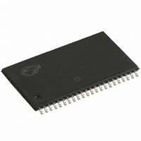
CY7C1041BV33-12ZC Cypress Semiconductor Corp, CY7C1041BV33-12ZC Datasheet

CY7C1041BV33-12ZC
Specifications of CY7C1041BV33-12ZC
Related parts for CY7C1041BV33-12ZC
CY7C1041BV33-12ZC Summary of contents
Page 1
... HIGH), the outputs are disabled (OE HIGH), the BHE and BLE are disabled (BHE, BLE HIGH), or during a write operation (CE LOW, and WE LOW). The CY7C1041BV33 is available in a standard 44-pin 400-mil-wide body width SOJ and 44-pin TSOP II package with center power and ground (revolutionary) pinout. ...
Page 2
... CE > > < MAX Max Com’l/Ind’ > V – 0.3V, CC Com’l V > V – 0.3V < 0.3V CY7C1041BV33 [1] ................................ –0. Ambient [2] Temperature +70 C 3.3V – +85 C -12 -15 Min. Max. Min. Max. 2.4 2.4 0.4 0.4 2 0.5 + 0.5 –0.5 0.8 –0.5 0.8 – ...
Page 3
... Com’l/Ind’ > V – 0.3V, CC Com’ > V – 0.3V < 0.3V, f=0 IN Test Conditions MHz VENIN EQUIVALENT 3.3V 167 1.73V (b) GND Rise time: 1 V/ns CY7C1041BV33 -17 -20 -25 Min. Max. Min. Max. Min. Max. 2.4 2.4 2.4 0.4 0 0.5 0.5 –0.5 0.8 – ...
Page 4
... The input data set-up and hold timing should be referenced to the leading edge of the signal that terminates the write. 8. The minimum write cycle time for Write Cycle No. 3 (WE controlled, OE LOW) is the sum of t Document #: 38-05168 Rev. ** Over the Operating Range Min less than less than t HZCE LZCE HZOE LZOE CY7C1041BV33 -12 -15 -17 Max. Min. Max. Min. Max ...
Page 5
... No input may exceed V + 0.5V. CC Document #: 38-05168 Rev. ** Over the Operating Range (continued) Min Over the Operating Range (For L version only) Conditions 2.0V > V – 0.3V > V – 0. CY7C1041BV33 -20 -25 Max. Min. Max [10] Min ...
Page 6
... Address valid prior to or coincident with CE transition LOW. Document #: 38-05168 Rev. ** DATA RETENTION MODE 3.0V V > CDR OHA [12, 13 ACE t DOE t LZOE t DBE t LZBE 50 CY7C1041BV33 3. DATA VALID t HZOE t HZCE t HZBE IMPEDANCE DATA VALID t PD 50% 1041BV33– 1041BV33-6 HIGH I ICC CC I ISB SB 1041BV33-7 Page ...
Page 7
... Write Cycle No. 2 (BLE or BHE Controlled) ADDRESS t SA BHE, BLE WE CE DATAI/O Notes: 14. Data I/O is high-impedance BHE and/or BLE goes HIGH simultaneously with WE going HIGH, the output remains in a high–impedance state. Document #: 38-05168 Rev. ** [14, 15 SCE PWE PWE t SCE . IH CY7C1041BV33 1041BV33 1041BV33-9 Page ...
Page 8
... High Z High Z Data Out Data Out Data Out High Z High Z Data Out Data In Data In Data In High Z High Z Data In High Z High Z CY7C1041BV33 LZWE Mode Power Down Standby (I Read All Bits Active (I Read Lower Bits Only Active (I Read Upper Bits Only Active (I ...
Page 9
... Ordering Information Speed (ns) Ordering Code 12 CY7C1041BV33-12VC CY7C1041BV33L-12VC CY7C1041BV33-12ZC CY7C1041BV33L-12ZC 15 CY7C1041BV33-15VC CY7C1041BV33L-15VC CY7C1041BV33-15ZC CY7C1041BV33L-15ZC CY7C1041BV33-15VI CY7C1041BV33-15ZI 17 CY7C1041BV33-17VC CY7C1041BV33L-17VC CY7C1041BV33-17ZC CY7C1041BV33L-17ZC CY7C1041BV33-17VI CY7C1041BV33-17ZI 20 CY7C1041BV33-20VC CY7C1041BV33L-20VC CY7C1041BV33-20ZC CY7C1041BV33L-20ZC CY7C1041BV33-20VI CY7C1041BV33-20ZI 25 CY7C1041BV33-25VC CY7C1041BV33L-25VC CY7C1041BV33-25ZC CY7C1041BV33L-25ZC CY7C1041BV33-25VI CY7C1041BV33-25ZI Document #: 38-05168 Rev. ** Package Name Package Type V34 ...
Page 10
... The inclusion of Cypress Semiconductor products in life-support systems application implies that the manufacturer assumes all risk of such use and in doing so indemnifies Cypress Semiconductor against all charges. 44-Lead (400-Mil) Molded SOJ V34 44-Pin TSOP II Z44 CY7C1041BV33 51-85082-B 51-85087-A Page ...
Page 11
... Document Title: CY7C1041BV33 256K x 16 SRAM Document Number: 38-05168 Issue REV. ECN NO. Date ** 111840 11/17/01 Document #: 38-05168 Rev. ** Orig. of Change DSG Change from Spec number: 38-00932 to 38-05168 CY7C1041BV33 Description of Change Page ...


