CY7C128A-35PC Cypress Semiconductor Corp, CY7C128A-35PC Datasheet
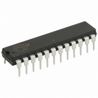
IC SRAM 16KBIT 35NS 24DIP

CY7C128A-35PC

Manufacturer Part Number
CY7C128A-35PC
Description
IC SRAM 16KBIT 35NS 24DIP
Manufacturer
Cypress Semiconductor Corp
Datasheet

Specifications of CY7C128A-35PC

Format - Memory
RAM
Memory Type
SRAM - Asynchronous
Memory Size
16K (2K x 8)
Speed
35ns
Interface
Parallel
Voltage - Supply
4.5 V ~ 5.5 V
Operating Temperature
0°C ~ 70°C
Package / Case
24-DIP (0.300", 7.62mm)
Lead Free Status / RoHS Status
Contains lead / RoHS non-compliant
Other names
428-1045

Available stocks

Company
Part Number
Manufacturer
Quantity
Price
Part Number:
CY7C128A-35PC
Manufacturer:
CY31
Quantity:
81
Part Number:
CY7C128A-35PC
Quantity:
200
Part Number:
CY7C128A-35PC
Manufacturer:
CYPRESS/赛普拉斯
Quantity:
20 000
Company:
Part Number:
CY7C128A-35PC
Quantity:
216
Company:
Part Number:
CY7C128A-35PC
Quantity:
199
28A
Cypress Semiconductor Corporation
Document #: 38-05028 Rev. **
Features
Functional Description
The CY7C128A is a high-performance CMOS static RAM or-
ganized as 2048 words by 8 bits. Easy memory expansion is
Selection Guide
Maximum Access Time (ns)
Maximum Operating
Current (mA)
Maximum Standby
Current (mA)
• Automatic power-down when deselected
• CMOS for optimum speed/power
• High speed
• Low active power
• Low standby power
• TTL-compatible inputs and outputs
• Capable of withstanding greater than 2001V electro-
• V
static discharge
— 15 ns
— 660 mW (commercial)
— 688 mW (military—20 ns)
— 110 mW (20 ns)
IH
Logic Block Diagram
CE
WE
OE
of 2.2V
A
A
A
A
A
A
A
10
9
8
7
6
5
4
A
3
INPUT BUFFER
128 x 16 x 8
DECODER
COLUMN
ARRAY
A
2
Commercial
Military
Commercial
Military
A
1
A
0
POWER
DOWN
3901 North First Street
7C128A-15
120
15
40
-
-
provided by an active LOW Chip Enable (CE), and active LOW
Output Enable (OE) and three-state drivers. The CY7C128A
has an automatic power-down feature, reducing the power
consumption by 83% when deselected.
Writing to the device is accomplished when the Chip Enable
(CE) and Write Enable (WE) inputs are both LOW.
Data on the eight I/O pins (I/O
memory location specified on the address pins (A
A
Reading the device is accomplished by taking Chip Enable
(CE) and Output Enable (OE) LOW while Write Enable (WE)
remains HIGH. Under these conditions, the contents of the
memory location specified on the address pins will appear on
the eight I/O pins.
The I/O pins remain in high-impedance state when Chip En-
able (CE) or Output Enable (OE) is HIGH or Write Enable (WE)
is LOW.
The CY7C128A utilizes a die coat to insure alpha immunity.
7C128A-20
10
).
C128A–1
120
125
I/O
I/O
I/O
I/O
I/O
I/O
I/O
I/O
20
20
20
0
1
2
3
4
5
6
7
San Jose
Pin Configurations
7C128A-25
120
125
25
20
20
2K x 8 Static RAM
I/O
I/O
GND
I/O
I/O
I/O
A
A
A
A
A
CA 95134
A
A
A
A
A
A
A
A
0
4
3
2
1
0
0
1
7
6
5
4
3
2
1
0
0
1
2
through I/O
7C128A-35
4
5
6
7
8
9
10
1
2
3
4
5
6
7
8
9
10
11
12
DIP/SOJ/SOIC
Top View
11 12 13 14 15
Top View
3 2 1
7C128A
7C128A
LCC
Revised August 24, 2001
120
125
35
20
20
24
24
23
22
21
20
19
18
17
16
15
14
13
23
CY7C128A
7
22
21
20
19
18
17
16
) is written into the
WE
V
A
A
OE
A
CE
I/O
I/O
I/O
I/O
I/O
CC
8
9
10
A
WE
OE
A
CE
I/O
I/O
7
6
5
4
3
9
10
408-943-2600
C128A–2
C128A–3
7
6
7C128A-45
120
125
0
45
20
20
through
[+] Feedback

Related parts for CY7C128A-35PC

CY7C128A-35PC Summary of contents

Page 1

... I/O pins. The I/O pins remain in high-impedance state when Chip En- able (CE) or Output Enable (OE) is HIGH or Write Enable (WE) is LOW. The CY7C128A utilizes a die coat to insure alpha immunity. I/O I/O I/O I/O ...

Page 2

... I CC < V –10 +10 – –300 Com’l 120 Mil - , Com’l 40 Mil - , Com’l 40 –0.3V, –0.3V Mil - Test Conditions MHz 5.0V CC CY7C128A Ambient Temperature + 10% – +125 C 5V 10% 7C128A-25 7C128A-35,45 Min. Max. Unit 2.4 2.4 V 0.4 0.4 0 2 0.8 –0.5 0.8 – ...

Page 3

... GND 255 JIG AND (b) SCOPE C128A–4 [2, 6] 7C128A-15 7C128A-20 7C128A-25 Min. Max. Min. Max. Min less than t for any given device. HZCE LZCE CY7C128A ALL INPUT PULSES 90% 90% 10% 10 C128A–5 7C128A-35 7C128A-45 Max. Min. Max. Min. Max. Unit ...

Page 4

... Data I/O pins enter high-impedance state, as shown, when OE is held LOW during write. Document #: 38-05028 Rev OHA DOE DATA VALID 50 SCE PWE t SD DATA VALID IN t HZWE CY7C128A DATA VALID C128A–6 t HZOE t HZCE HIGH IMPEDANCE 50 C128A– LZWE HIGH IMPEDANCE C128A–8 Page [+] Feedback ...

Page 5

... 5. 0.0 –55 25 125 AMBIENT TEMPERATURE( C) NORMALIZED ACCESS TIME vs. AMBIENT TEMPERATURE 1.6 1.4 1.2 1 5.0V CC 0.8 0.6 –55 25 125 AMBIENT TEMPERATURE( C) CY7C128A C128A–9 OUTPUT SOURCE CURRENT vs. OUTPUT VOLTAGE 120 100 80 V =5. 0.0 1.0 2.0 3.0 4.0 OUTPUT VOLTAGE(V) OUTPUT SINK CURRENT vs ...

Page 6

... SUPPLY VOLTAGE(V) Ordering Information Speed (ns) Ordering Code 15 CY7C128A-15PC CY7C128A-15VC CY7C128A-15SC 20 CY7C128A-20PC CY7C128A-20VC CY7C128A-20SC CY7C128A-20DMB CY7C128A-20LMB 25 CY7C128A-25PC CY7C128A-25VC CY7C128A-25SC CY7C128A-25DMB 35 CY7C128A-35PC CY7C128A-35VC CY7C128A-35SC CY7C128A-35DMB 45 CY7C128A-45PC CY7C128A-45VC CY7C128A-45SC CY7C128A-45DMB CY7C128A-45LMB Document #: 38-05028 Rev. ** TYPICAL ACCESS TIME CHANGE vs. OUTPUT LOADING 30.0 25.0 20.0 15.0 10 4.5V CC ...

Page 7

... MILITARY SPECIFICATIONS Group A Subgroup Testing DC Characteristics Parameter Subgroups Max Switching Characteristics Parameter Subgroups READ CYCLE 10 10 10, 11 OHA 10, 11 ACE 10, 11 DOE WRITE CYCLE 10 10, 11 SCE 10, 11 PWE 10 10 Document #: 38-05028 Rev. ** CY7C128A Page [+] Feedback ...

Page 8

... Package Diagrams 24-Pin Rectangular Leadless Chip Carrier L53 Document #: 38-05028 Rev. ** 24-Lead (300-Mil) CerDIP D14 MIL-STD-1835 D- 9 Config.A 51-80066 CY7C128A 51-80031 Page [+] Feedback ...

Page 9

... The inclusion of Cypress Semiconductor products in life-support systems application implies that the manufacturer assumes all risk of such use and in doing so indemnifies Cypress Semiconductor against all charges. 24-Lead (300-Mil) Molded DIP P13/P13A 24-Lead (300-Mil) Molded SOJ V13 CY7C128A 51-85013-A 51-85030-A Page ...

Page 10

... Document Title: CY7C128A Static RAM Document Number: 38-05028 Issue Orig. of REV. ECN NO. Date Change ** 106814 09/10/01 SZV Document #: 38-05028 Rev. ** Description of Change Change from Spec number: 38-00094 to 38-05028 CY7C128A Page [+] Feedback ...

Related keywords