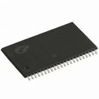
CY7C1041CV33-15ZC Cypress Semiconductor Corp, CY7C1041CV33-15ZC Datasheet

CY7C1041CV33-15ZC
Specifications of CY7C1041CV33-15ZC
Available stocks
Related parts for CY7C1041CV33-15ZC
CY7C1041CV33-15ZC Summary of contents
Page 1
... HIGH), the outputs are disabled (OE HIGH), the BHE and BLE are disabled (BHE, BLE HIGH), or during a Write operation (CE LOW, and WE LOW). The CY7C1041CV33 is available in a standard 44-pin 400-mil-wide body width SOJ and 44-pin TSOP II package with center power and ground (revolutionary) pinout, as well as a 48-ball fine-pitch ball grid array (FBGA) package ...
Page 2
... Maximum Operating Current Maximum CMOS Standby Current Pin Configurations Document #: 38-05134 Rev. *H -10 10 Commercial 90 Industrial 100 Automotive-A 100 Automotive-E Commercial/ 10 Industrial Automotive-A 10 Automotive-E 48-ball FBGA (Top View BLE I BHE I I/O I I/O I I/O I I/O I CY7C1041CV33 -12 - Unit Page ...
Page 3
... When LOW, the I/O pins are allowed to behave as outputs. When deasserted HIGH, I/O pins are tri-stated, and act as input data pins. D1, E6 Ground Ground for the device. Should be connected to ground of the system. D6, E1 Power Supply Power Supply inputs to the device. CY7C1041CV33 Description , BLE controls I/O –I Page ...
Page 4
... CC Auto-A 10 > V – 0.3V, CC < 0.3V Auto-E IN Test Conditions T = 25° MHz CY7C1041CV33 Ambient Temperature 0°C to +70°C –40°C to +85°C –40°C to +85°C –40°C to +125°C -12 -15 Max. Min. Max. Min. Max. 2.4 2.4 2.4 0.4 ...
Page 5
... CC is less than less than t HZCE LZCE HZOE CY7C1041CV33 TSOP-II FBGA 42.96 38.15 10.75 9.15 R 317Ω R2 351Ω High-Z Characteristics R 317Ω 3.3V OUTPUT 5 pF (d) -15 -20 Max. Min. Max. Min. Max. 100 100 ...
Page 6
... Address valid prior to or coincident with CE transition LOW. Document #: 38-05134 Rev. *H [5] Over the Operating Range (continued) -10 -12 Min. Max. Min OHA ACE t DOE t LZOE t DBE t LZBE 50 CY7C1041CV33 -15 -20 Max. Min. Max. Min. Max DATA VALID t HZOE t HZCE t HZBE IMPEDANCE DATA VALID t PD 50% and t . HZWE SD Unit ...
Page 7
... Write Cycle No. 2 (BLE or BHE Controlled) ADDRESS t SA BHE, BLE WE CE DATA I/O Notes: 14. Data I/O is high-impedance BHE and/or BLE = V 15 goes HIGH simultaneously with WE going HIGH, the output remains in a high-impedance state. Document #: 38-05134 Rev SCE PWE PWE t SCE CY7C1041CV33 Page ...
Page 8
... High-Z High-Z Data Out Data Out Data Out High-Z High-Z Data Out Data In Data In Data In High-Z High-Z Data In High-Z High-Z CY7C1041CV33 LZWE Mode Power-down Standby (I Read All Bits Active (I Read Lower Bits Only Active (I Read Upper Bits Only Active (I Write All Bits ...
Page 9
... CY7C1041CV33-10BAXI CY7C1041CV33-10ZI CY7C1041CV33-10ZXI CY7C1041CV33-10ZSXA CY7C1041CV33-10BAXA 12 CY7C1041CV33-12VC CY7C1041CV33-12VXC CY7C1041CV33-12ZC CY7C1041CV33-12ZXC CY7C1041CV33-12VXI CY7C1041CV33-12ZI CY7C1041CV33-12ZXI 15 CY7C1041CV33-15VC CY7C1041CV33-15VXC CY7C1041CV33-15ZC CY7C1041CV33-15ZXC CY7C1041CV33-15VI CY7C1041CV33-15VXI CY7C1041CV33-15ZI CY7C1041CV33-15ZXI 20 CY7C1041CV33-20ZC CY7C1041CV33-20ZXC CY7C1041CV33-20ZSXA CY7C1041CV33-20VE CY7C1041CV33-20VXE CY7C1041CV33-20ZE CY7C1041CV33-20ZSXE Please contact your local Cypress sales representative for availability of these parts Document #: 38-05134 Rev. *H ...
Page 10
... Package Diagrams 48-Ball (7. 8 1.2 mm) FBGA (51-85106) TOP VIEW A1 CORNER 7.00±0.10 SEATING PLANE C Document #: 38-05134 Rev. *H CY7C1041CV33 BOTTOM VIEW A1 CORNER Ø0. Ø0. Ø0.30±0.05(48X 1.875 A 0.75 3.75 B 7.00±0.10 0.15(4X) 51-85106-*E Page ...
Page 11
... The inclusion of Cypress products in life-support systems application implies that the manufacturer assumes all risk of such use and in doing so indemnifies Cypress against all charges. 44-lead (400-mil) Molded SOJ (51-85082) 44-pin TSOP II (51-85087) CY7C1041CV33 51-85082-*B 51-85087-*A Page ...
Page 12
... Document History Page Document Title: CY7C1041CV33 4-Mbit (256K x 16) Static RAM Document Number: 38-05134 REV. ECN NO. Issue Date ** 109513 12/13/01 *A 112440 12/20/01 *B 112859 03/25/02 *C 116477 09/16/02 *D 119797 10/21/02 *E 262949 See ECN *F 361795 See ECN *G 435387 See ECN *H 499153 See ECN Document #: 38-05134 Rev. *H Orig ...


