CY7C199C-12VC Cypress Semiconductor Corp, CY7C199C-12VC Datasheet
CY7C199C-12VC
Specifications of CY7C199C-12VC
Available stocks


Related parts for CY7C199C-12VC


CY7C199C-12VC Summary of contents
Page 1
... Cypress Semiconductor Corporation Document #: 38-05408 Rev. *C 256K (32K x 8) Static RAM General Description The CY7C199C is a high-performance CMOS Asynchronous SRAM organized as 32K by 8 bits that supports an asynchronous memory interface. The device features an automatic power-down feature that significantly reduces power consumption when deselected. ...
Page 2
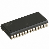
... Pin Layout and Specifications Document #: 38-05408 Rev DIP (6.9 x 35.6 x 3 TSOP 13.4 mm) 28 SOJ CY7C199C Page ...
Page 3
... CC = Max mA, OUT = 1/t MAX ≥ V ≥ ≤ MAX ≥ V – 0.3V ≥ V ≤ – 0.3V CY7C199C SOJ TSOP 10, 11, 12, 21, 23, 24, 25, 26 13, 14, 15, 16, 17 18, 19, 20, 22, 23, 24, 25 Value –65 to +150 –55 to +125 –0.5 to +7.0 –0 0 > 2001 > 200 ) Voltage Range (V CC 5.0V ± ...
Page 4
... CC Conditions Still Air, soldered × 4.5 square inch, two–layer printed circuit board INCLUDING JIGAND SCOPE ( HZOE, HZCE, HZWE CY7C199C Max. ALL – PACKAGES 8 8 TSOP I SOJ DIP 88.6 79 69.33 21.94 41.42 31.62 ALL INPUT PULSES 3.0V 90% 90% 10% GND ≤ 1V/ns Equivalent to: THÉ ...
Page 5
... A/C Test Loads. Transitions are measured ± 200 mV from steady state voltage. HZOE HZCE HZWE Document #: 38-05408 Rev. *C Description [ Min Max less than less than t HZCE LZCE HZOE CY7C199C Nom 480 255 167 1. Min Max Min Max ...
Page 6
... Device is continuously selected CE HIGH for Read Cycle. Document #: 38-05408 Rev. *C [8] Condition =2.0V, CE ≥ – 0.3V ≥ V ≤ 0.3V V – 0. DATA RETENTION MODE OHA CY7C199C ALL Min. Max. Unit 2.0 – V µA – 150 0 – ns µs 200 – Data Valid Page ...
Page 7
... This cycle is WE controlled HIGH during write. 14. Data In/Out is high impedance 15. During this period the I/Os are in output state and input signals should not be applied. Document #: 38-05408 Rev ACE t DOE t LZOE t LZCE SCE Data-In Valid CY7C199C t HZCE t HZOE Data Valid 50 PWE High Page ...
Page 8
... If CE goes HIGH simultaneously with WE going HIGH, the output remains in a high-impedance state. 18. The cycle is WE controlled, OE LOW. The minimum write cycle time is the sum of t Document #: 38-05408 Rev SCE Data-In Valid [18 SCE PWE t SD Data-In Valid t HZWE and t . HZWE SD CY7C199C High Undefined See Footnotes t LZWE Page ...
Page 9
... Ordering Code 12 CY7C199C–12VC CY7C199C–12VXC CY7C199C–12ZXC CY7C199C–12VI 15 CY7C199C–15PC CY7C199C–15PXC CY7C199C–15ZC CY7C199C–15ZXC CY7C199C–15VC CY7C199C–15VXC CY7C199CL–15VC CY7C199CL–15VXC CY7C199C–15VI 20 CY7C199C–20ZXI Document #: 38-05408 Rev. *C Input/Output High Z Deselect/Power-Down Data Out Read Data In Write ...
Page 10
... Package Diagrams Document #: 38-05408 Rev. *C 28-pin TSOP 13.4 mm) (51-85071) CY7C199C 51-85071-*G Page ...
Page 11
... A 0.050 TYP. Document #: 38-05408 Rev. *C 28-pin (300-Mil) Molded SOJ (51-85031) PIN 0.291 0.330 0.300 0.350 28 SEATING PLANE 0.120 0.140 0.004 0.025 MIN. CY7C199C A DETAIL EXTERNAL LEAD DESIGN 0.026 0.032 0.013 0.019 0.014 0.020 OPTION 1 OPTION 2 0.007 0.013 0.262 0.272 51-85031-*C Page ...
Page 12
... SEATING PLANE 1.345[34.16] 1.385[35.18] 0.120[3.05] 0.140[3.55] 0.015[0.38] 0.060[1.52] 0.055[1.39] 0.065[1.65] 0.015[0.38] 0.020[0.50] SEE LEAD END OPTION CY7C199C DIMENSIONS IN INCHES [MM] MIN. MAX. REFERENCE JEDEC MO-095 PACKAGE WEIGHT: 2.15 gms 0.290[7.36] 0.325[8.25] 0.009[0.23] 3° MIN. 0.012[0.30] 0.310[7.87] 0.385[9.78] 51-85014-*D Page ...
Page 13
... Document History Page Document Title: CY7C199C 256K (32K x 8) Static RAM Document Number: 38-05408 Issue REV. ECN No. Date ** 129233 09/11/03 *A 129697 09/15/03 *B 341574 See ECN *C 492500 See ECN Document #: 38-05408 Rev. *C Orig. of Change Description of Change HGK New Data Sheet KKV Minor change: ...