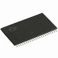
CY7C1041B-15ZXC Cypress Semiconductor Corp, CY7C1041B-15ZXC Datasheet

CY7C1041B-15ZXC
Specifications of CY7C1041B-15ZXC
Available stocks
Related parts for CY7C1041B-15ZXC
CY7C1041B-15ZXC Summary of contents
Page 1
... TTL-compatible inputs and outputs • Easy memory expansion with CE and OE features Functional Description The CY7C1041B is a high-performance CMOS static RAM organized as 262,144 words by 16 bits. Writing to the device is accomplished by taking Chip Enable (CE) and Write Enable (WE) inputs LOW. If Byte Low Enable ...
Page 2
... CC = Max., Com’l = 1/t MAX RC Ind’ > > < MAX , Com’l CC – 0.3V, CC Com’l L > V – 0.3V, CC < 0.3V Ind’l IN CY7C1041B Unit 170 160 mA 190 180 0.5 0 [1] ................................ –0. 0.5V CC Ambient [2] Temperature V CC 0°C to +70°C 5V ± 0.5 –40°C to +85°C ...
Page 3
... Com’ > V – 0.3V, CC Com’ > V – 0.3V Ind’ < 0.3V Test Conditions T = 25° MHz 5. 481 Ω 5V 3.0V R2 GND 5 pF 255Ω ≤ (b) CY7C1041B 7C1041B-25 Max. Min. Max. Unit 2.4 V 0.4 0 0 0.8 –0.5 0 – – 170 ...
Page 4
... The minimum write cycle time for Write Cycle no. 3 (WE controlled, OE LOW) is the sum of t Document #: 38-05142 Rev. *A 7C1041B-12 Min. Max. Min. [ time has to be provided initially before a read/write operation is power is less than less than t , and t HZCE LZCE HZOE LZOE HZWE and t HZWE CY7C1041B 7C1041B-15 7C1041B-17 Max. Min. Max. Unit µ ...
Page 5
... No input may exceed V + 0.5V. CC Document #: 38-05142 Rev. *A 7C1041B-20 Min. [ Over the Operating Range (L version only) [11] Conditions Com’ 3.0V > V – 0.3V > V – 0. CY7C1041B 7C1041B-25 Max. Min. Max. Unit µ ...
Page 6
... Device is continuously selected. OE, CE, BHE, and/or BHE = V 13 HIGH for read cycle. 14. Address valid prior to or coincident with CE transition LOW. Document #: 38-05142 Rev. *A DATA RETENTION MODE 3.0V V > CDR OHA t RC DOE DATA VALID 50 CY7C1041B 3. DATA VALID t HZOE t HZCE t HZBE HIGH IMPEDANCE t PD ICC 50% ISB Page [+] Feedback ...
Page 7
... Write Cycle No. 2 (BLE or BHE Controlled) ADDRESS t SA BHE, BLE WE CE DATAI/O Notes: 15. Data I/O is high impedance BHE and/or BLE goes HIGH simultaneously with WE going HIGH, the output remains in a high-impedance state. Document #: 38-05142 Rev SCE PWE PWE t SCE CY7C1041B Page [+] Feedback ...
Page 8
... Power Down Data Out Read All bits High Z Read Lower bits only Data Out Read Upper bits only Data In Write All bits High Z Write Lower bits only Data In Write Upper bits only High Z Selected, Outputs Disabled CY7C1041B LZWE Mode Power Standby ( Active ( ...
Page 9
... Ordering Information Speed (ns) Ordering Code 12 CY7C1041B-12VC CY7C1041B-12VXC CY7C1041B-12ZC CY7C1041B-12ZXC 15 CY7C1041B-15VC CY7C1041B-15VXC CY7C1041BL-15VC CY7C1041B-15ZC CY7C1041B-15ZXC CY7C1041BL-15ZC CY7C1041BL-15ZXC 17 CY7C1041B-17VC CY7C1041BL-17VC CY7C1041B-17ZC CY7C1041BL-17ZC 20 CY7C1041B-20VC CY7C1041B-20VXC CY7C1041BL-20VC CY7C1041BL-20VXC CY7C1041B-20ZC CY7C1041B-20ZXC CY7C1041BL-20ZC 25 CY7C1041B-25VC CY7C1041BL-25VC CY7C1041B-25ZC CY7C1041BL-25ZC 15 CY7C1041B-15ZI CY7C1041B-15ZXI CY7C1041B-15VI CY7C1041B-15VXI 17 CY7C1041B-17ZI CY7C1041B-17VI 20 CY7C1041B-20ZI CY7C1041B-20ZXI CY7C1041B-20VI CY7C1041B-20VXI ...
Page 10
... The inclusion of Cypress products in life-support systems application implies that the manufacturer assumes all risk of such use and in doing so indemnifies Cypress against all charges. 44-Lead (400-Mil) Molded SOJ V34 44-Pin TSOP II Z44 CY7C1041B 51-85082-*B 51-85087-*A Page ...
Page 11
... Document History Page Document Title: CY7C1041B 256K x 16 Static RAM Document Number: 38-05142 Issue Orig. of REV. ECN NO. Date Change ** 109886 09/15/01 SZV *A 341401 See ECN AJU Document #: 38-05142 Rev. *A Description of Change Change from Spec number: 38-00938 to 38-05142 Added Pb-free ordering information ...


