CY7C056V-12AXC Cypress Semiconductor Corp, CY7C056V-12AXC Datasheet
CY7C056V-12AXC
Specifications of CY7C056V-12AXC
Available stocks


Related parts for CY7C056V-12AXC


CY7C056V-12AXC Summary of contents
Page 1
... CY7C056V CY7C057V CY7C037V CY7C038V3.3 V 16K/32K x 36 FLEx36™ Asynchronous Dual-Port Static RAM Features True dual-ported memory cells that allow simultaneous ■ access of the same memory location 16K x 36 organization (CY7C056V) ■ 32K x 36 organization (CY7C057V) ■ 0.25-micron Complimentary metal oxide semiconductor ■ ...
Page 2
... Bus Match Operation ..................................................... 20 Long-Word (36-bit) Operation ................................... 21 Word (18-bit) Operation ............................................. 21 Byte (9-bit) Operation ................................................ 21 Ordering Information ...................................................... 22 Ordering Code Definition ........................................... 22 Package Diagrams .......................................................... 23 Acronyms ........................................................................ 24 Document Conventions ................................................. 24 Units of Measure ....................................................... 24 Sales, Solutions, and Legal Information ...................... 26 Worldwide Sales and Design Support ....................... 26 Products .................................................................... 26 PSoC Solutions ......................................................... 26 CY7C056V CY7C057V Page [+] Feedback ...
Page 3
... Functional Description The CY7C056V and CY7C057V are low-power CMOS 16K and 32K x 36 dual-port static RAMs. Various arbitration schemes are included on the devices to handle situations when multiple processors access the same piece of data. Two ports are provided, permitting independent, asynchronous access for reads and writes to any location in memory ...
Page 4
... A12L 31 A13L 32 [ I/O26L 34 I/O25L 35 I/O24L 36 Notes 4. This pin is A14L for CY7C057V. 5. This pin is A14R for CY7C057V Document #: 38-06055 Rev. *E CY7C056V (16K x 36) CY7C057V (32K x 36) CY7C056V CY7C057V 108 I/O33R I/O34R 107 106 I/O35R 105 A0R 104 A1R 103 A2R 102 A3R ...
Page 5
... A5R A4R SIZE A7R A6R VDD CE0R BA WA OER CE1R A8R R/WR VSS VDD VDD A10R A9R SEMR NC A12R A11R INTR A13R BUSYR [5] I/O18R I/O22R NC NC I/O6R I/O8R I/O20R I/O24R VSS NC I/O21R I/O23R CY7C056V CY7C057V Unit - 240 A A Page [+] Feedback ...
Page 6
... Read/Write Enable Byte select inputs. Asserting these signals enables read and write operations to the corresponding bytes of the memory array. See bus matching for details. See bus matching for details. Master or Slave select Ground Power CY7C056V CY7C057V V and Page [+] Feedback ...
Page 7
... Output current into outputs (LOW) .............................. 20 mA Static discharge voltage........................................... >2001 V Latch-up current ..................................................... >200 mA +150 C Operating Range +125 C Range Commercial Industrial +0 [7] +0 CY7C056V CY7C057V Ambient Temperature V DD +70 C 3.3 V ± 165 mV – +85 C 3.3 V ± 165 mV Page [+] Feedback ...
Page 8
... Commercial 55 Industrial Commercial 180 – Industrial Commercial 0.01 Industrial Commercial 160 [9] Industrial Test Conditions MHz 3 LOW. 1 CY7C056V CY7C057V CY7C056V CY7C057V -15 Max Min Typ Max Unit – 2.4 – V 0.4 – 0.4 V – – 2.0 – V 0.8 – 0.8 V A 10 –10 ...
Page 9
... Notes 11. External AC Test Load Capacitance = 10 pF. 12. (Internal I/O pad Capacitance = 10 pF Test Load. Document #: 38-06055 Rev. *E OUTPUT = 1 (b) Three-State Delay (Load 2) 3.0 V 90% 10 [12 100 200 Capacitance (pF) (b) Load Derating Curve CY7C056V CY7C057V 3 590 435 90% 10% Page [+] Feedback ...
Page 10
... HZCE LZCE HZOE LZOE CY7C056V CY7C057V Unit -15 Max – – – – – – – ns – ns – ns – ...
Page 11
... SEM flag contention window SPS t SEM address access time SAA Data Retention Mode The CY7C056V and CY7C057V are designed with battery backup in mind. Data retention voltage and supply current are guaranteed over temperature. The following rules ensure data retention: [23] 1. Chip Enable (CE) ...
Page 12
... CHIP SELECT VALID t ACE t LZCE =V , and WA, BA are valid. This waveform cannot be used for semaphore reads transition HIGH WA, BA are valid, and SEM = access semaphore CY7C056V CY7C057V [25, 26, 27] t OHA [25, 28, 29] t HZCE t HZOE DATA VALID OHA t HZCE t HZCE = and SEM = ...
Page 13
... Document #: 38-06055 Rev CHIP SELECT VALID [33] t PWE [36] t HZWE CHIP SELECT VALID t SCE and SEM=V and B LOW 0– PWE . CY7C056V CY7C057V [30, 31, 32, 33] [36] t HZOE LZWE NOTE [30, 31, 32, 38 allow the I/O drivers to turn off and data HZWE SD Page [+] Feedback ...
Page 14
... SPS Document #: 38-06055 Rev SAA VALID ADRESS SCE SOP t SD DATA VALID PWE t SWRD t SOP WRITE CYCLE READ CYCLE MATCH t SPS MATCH = CE = HIGH and =LOW CY7C056V CY7C057V [39] t OHA t ACE DATA VALID OUT t DOE [40, 41, 42] Page [+] Feedback ...
Page 15
... Timing Diagram of Write with BUSY (M/S = HIGH) ADDRESS R R/W R DATA ADDRESS L BUSY L DATA OUTL R/W BUSY Note 43 LOW HIGH Document #: 38-06055 Rev MATCH t PWE t SD VALID MATCH t BLA t Write Timing with Busy Input (M/S = LOW) t PWE CY7C056V CY7C057V [43 BHA t BDD t DDD VALID WDD Page [+] Feedback ...
Page 16
... BUSY will be asserted. PS Document #: 38-06055 Rev. *E ADDRESS MATCH CHIP SELECT VALID t PS CHIP SELECT VALID t BLC ADDRESS MATCH CHIP SELECT VALID t PS CHIP SELECT VALID t BLC ADDRESS MISMATCH t t BLA BHA ADDRESS MISMATCH t t BLA BHA CY7C056V CY7C057V [44] t BHC t BHC [44] Page [+] Feedback ...
Page 17
... Document #: 38-06055 Rev. *E Interrupt Timing Diagrams t WC [45 (7FFF for CY7C057V) CHIP SELECT VALID [46] t INR t WC [45 (7FFE for CY7C057V) CHIP SELECT VALID [46] t INR or R deasserted first. L / asserted last CY7C056V CY7C057V t RC READ 3FFF t RC READ 3FFE Page [+] Feedback ...
Page 18
... Architecture The CY7C056V and CY7C057V consist of an array of 16K and 32K words of 36 bits each of dual-port RAM cells, I/O and address lines, and control signals (CE /CE 0 control pins permit independent access for reads or writes to any location in memory. To handle simultaneous writes/reads to the same location, a BUSY pin is provided on each port ...
Page 19
... Right port has semaphore token 1 1 Semaphore free 0 1 Left port has semaphore token 1 1 Semaphore free CY7C056V CY7C057V Operation Deselected: Power-down Deselected: Power-down Write to selected bytes only Write to all bytes Read selected bytes only Read all bytes Outputs disabled Read data in semaphore flag ...
Page 20
... The data sequencing arrangement is selected using the word address (WA) and byte address (BA) input pins. A logic “0” applied to both the bus match select (BM) CY7C056V CY7C057V I/O Pins Used I/O 0– ...
Page 21
... When transferring data in byte (9-bit) bus match format, the unused I/O 9R–35R CY7C056V CY7C057V . The level applied to the word address (WA) ). pins are three-stated. 18R–35R ...
Page 22
... X X Operating Range C = Com m ercial I = Industrial free (RoHS Com pliant) Package: A=TQFP or BB=FBGA Speed Grade : 12ns/15ns 3.3 V Depth: 6=16K or 7=32K W idth: 05=x36 7C = Dual Port SRAM Com pany ID Cypress CY7C056V CY7C057V Operating Range Commercial Operating Range Commercial Commercial Industrial Industrial Page [+] Feedback ...
Page 23
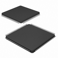
... Package Diagrams Figure 3. 144-Pin Plastic Thin Quad Flat Pack (TQFP) A144 Document #: 38-06055 Rev. *E CY7C056V CY7C057V 51-85047 *C Page [+] Feedback ...
Page 24
... BGA ball grid array Document #: 38-06055 Rev. *E 51-85114 *C Document Conventions Units of Measure Symbol Unit of Measure ns nano seconds V Volts µA micro Amperes mA milli Amperes Ohms mV milli Volts MHz Mega Hertz pF pico Farad W Watts °C degree Celcius CY7C056V CY7C057V Page [+] Feedback ...
Page 25
... SZV Change from Spec number: 38-00742 to 38-06055 RBI Power up requirements added to Maximum Ratings Information YIM Added Pb-Free Logo Added Pb-Free parts to ordering information: CY7C056V-12AXC, CY7C056V-15AXC, CY7C057V-12AXC, CY7C057V-15AXC, CY7CO57V-15AXI RAME Updated Ordering Information Updated Package Diagrams ADMU Removed part CY7C057V-15BBC Added part CY7C057V-15AXI ...
Page 26
... Cypress against all charges. Use may be limited by and subject to the applicable Cypress software license agreement. Document #: 38-06055 Rev. *E All products and company names mentioned in this document may be the trademarks of their respective holders. cypress.com/go/plc Revised March 30, 2011 CY7C056V CY7C057V PSoC Solutions psoc.cypress.com/solutions PSoC 1 | ...