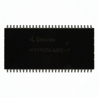
HYB39S256160FE-7 Qimonda, HYB39S256160FE-7 Datasheet - Page 6

HYB39S256160FE-7
Manufacturer Part Number
HYB39S256160FE-7
Description
IC SDRAM 256MBIT 143MHZ 54TSOP
Manufacturer
Qimonda
Datasheet
1.HYB39S256800FE-7.pdf
(27 pages)
Specifications of HYB39S256160FE-7
Format - Memory
RAM
Memory Type
SDRAM
Memory Size
256M (16Mx16)
Speed
143MHz
Interface
Parallel
Voltage - Supply
3 V ~ 3.6 V
Operating Temperature
0°C ~ 70°C
Package / Case
54-TSOP II
Lead Free Status / RoHS Status
Lead free / RoHS Compliant
Other names
675-1004-2
Available stocks
Company
Part Number
Manufacturer
Quantity
Price
Company:
Part Number:
HYB39S256160FE-7
Manufacturer:
FREESCALE
Quantity:
65
Company:
Part Number:
HYB39S256160FE-7
Manufacturer:
QIMONDA
Quantity:
7 298
2
This chapter contains the pin configuration table, the TSOP and FBGA package drawing, and the block diagrams for the ×4,
×8, ×16 organization of the SDRAM.
2.1
Listed below are the pin configurations sections for the various signals of the SDRAM.
Rev. 1.42, 2007-09
03292006-TMTK-JFEU
Ball No.
Clock Signals ×4/×8/×16 Organization
38,2F
37, 3F
Control Signals ×4/×8/×16 Organization
18, 8F
17, 7F
16, 9F
19, 9G
Address Signals ×4/×8/×16 Organization
20, 7G
21, 8G
23, 7H
24, 8H
25, 8J
26, 7J
29, 3J
30, 2J
31, 3H
32, 2H
33, 1H
34, 3G
22, 9H
35, 2G
36, 1G
Name
CLK
CKE
RAS
CAS
WE
CS
BA0
BA1
A0
A1
A2
A3
A4
A5
A6
A7
A8
A9
A10
A11
A12
Pin
Type
I
I
I
I
I
I
I
I
I
I
I
I
I
I
I
I
I
I
I
I
I
Configuration
Pin Description
Buffer
Type
LVTTL
LVTTL
LVTTL
LVTTL
LVTTL
LVTTL
LVTTL
LVTTL
LVTTL
LVTTL
LVTTL
LVTTL
LVTTL
LVTTL
LVTTL
LVTTL
LVTTL
LVTTL
LVTTL
LVTTL
LVTTL
Function
Clock Signal CK
Clock Enable
Row Address Strobe (RAS), Column Address Strobe (CAS), Write Enable (WE)
Chip Select
Bank Address Signals 1:0
Address Signal 12:0, Address Signal 10/Auto precharge
6
HY[B/I]39S256[40/80/16][0/7]F[E/T/F](L)
Pin Configuration of the SDRAM
256-MBit Synchronous DRAM
Internet Data Sheet
TABLE 4


