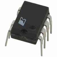
LNK500PN Power Integrations, LNK500PN Datasheet - Page 3

LNK500PN
Manufacturer Part Number
LNK500PN
Description
IC SWIT OCP CV/CC HV 8DIP
Manufacturer
Power Integrations
Series
LinkSwitch®r
Datasheet
1.LNK500PN.pdf
(20 pages)
Specifications of LNK500PN
Output Isolation
Isolated
Frequency Range
24 ~ 49.5kHz
Voltage - Output
700V
Power (watts)
4W
Operating Temperature
-40°C ~ 150°C
Package / Case
8-DIP (0.300", 7.62mm), 7 Leads
Output Voltage
5.6 V
Input / Supply Voltage (max)
265 VAC
Input / Supply Voltage (min)
85 VAC
Duty Cycle (max)
80 %
Switching Frequency
42 KHz
Supply Current
1.06 mA
Operating Temperature Range
- 40 C to + 150 C
Mounting Style
Through Hole
For Use With
596-1001 - KIT DESIGN ACCELERATOR ADAPTER
Lead Free Status / RoHS Status
Lead free / RoHS Compliant
Other names
596-1029-5
Available stocks
Company
Part Number
Manufacturer
Quantity
Price
Part Number:
LNK500PN
Manufacturer:
POWER
Quantity:
20 000
LinkSwitch Functional Description
The duty cycle, current limit and operating frequency
relationships with CONTROL pin current are shown in
Figure 4. Figure 5 shows a typical power supply outline
schematic which is used below to describe the LinkSwitch
operation.
Power Up
During power up, as V
pin capacitor C1 is charged through a switched high voltage
current source connected internally between the DRAIN and
CONTROL pins (see Figure 2). When the CONTROL pin
voltage reaches approximately 5.6 V relative to the SOURCE
pin, the high voltage current source is turned off, the internal
control circuitry is activated and the high voltage internal
MOSFET starts to switch. At this point, the charge stored on
C1 is used to supply the internal consumption of the chip.
Constant Current (CC) Operation
As the output voltage, and therefore the reflected voltage
across the primary transformer winding ramp up, the feedback
CONTROL current I
internal current limit increases with I
is equal to I
is designed to provide an approximately constant power supply
output current as the power supply output voltage rises.
Constant Voltage (CV) Operation
When I
duty cycle is reduced. At a value of I
supply input voltage, the duty cycle control limits LinkSwitch
peak current below the internal current limit value. At this point
the power supply transitions from CC to CV operation. With
minimum input voltage in a typical universal input design, this
transition occurs at approximately 30% duty cycle. Resistor R1
(Figure 5) is therefore initially selected to conduct a value of I
approximately equal to I
at the minimum power supply input voltage. The final choice
of R1 is made when the rest of the circuit design is complete.
When the duty cycle drops below approximately 4%, the
frequency is reduced, which reduces energy consumption under
light load conditions.
Auto-Restart Operation
When a fault condition, such as an output short circuit or open
loop, prevents flow of an external current into the CONTROL
pin, the capacitor C1 discharges towards 4.7 V. At 4.7 V, auto-
restart is activated, which turns the MOSFET off and puts the
control circuitry in a low current fault protection mode. In
auto-restart, LinkSwitch periodically restarts the power supply
so that normal power supply operation can be restored when
the fault is removed.
C
exceeds I
DCT
. The internal current limit vs. I
DCS
, typically 2 mA (Figure 4), the maximum
IN
C
is first applied (Figure 5), the CONTROL
increases. As shown in Figure 4, the
DCT
when V
OUT
C
C
and reaches I
that depends on power
is at the desired value
C
characteristic
LIM
when I
C
C
Figure 4. CONTROL Characteristics.
Figure 5. Power Supply Outline Schematic.
V
f
I
IN
LIM
OSC(low)
3.8%
Duty Cycle
Frequency
Internal Current Limit
77%
30%
f
OSC
Auto-restart
Auto-restart
Auto-restart
CONTROL Current I
CONTROL Current I
CONTROL Current I
LinkSwitch
D
I
CD1
C
R1
R2
D1
C1
S
C2
C
C
C
I
DCS
LNK500
C4
D2
PI-2799-112102
PI-2715-112102
2/05
I
D
DCT
V
OUT
3


