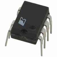
LNK306PN Power Integrations, LNK306PN Datasheet - Page 4

LNK306PN
Manufacturer Part Number
LNK306PN
Description
IC OFFLINE SWIT OCP 8DIP
Manufacturer
Power Integrations
Series
LinkSwitch®-TNr
Type
Off Line Switcherr
Datasheet
1.LNK302GN-TL.pdf
(20 pages)
Specifications of LNK306PN
Output Isolation
Non-Isolated
Frequency Range
62 ~ 70kHz
Voltage - Output
700V
Power (watts)
12mW
Operating Temperature
-40°C ~ 150°C
Package / Case
8-DIP (0.300", 7.62mm), 7 Leads
Output Voltage
12 V
Input / Supply Voltage (max)
265 VAC
Input / Supply Voltage (min)
85 VAC
Duty Cycle (max)
72 %
Switching Frequency
66 KHz
Supply Current
250 uA
Operating Temperature Range
- 40 C to + 150 C
Mounting Style
Through Hole
Lead Free Status / RoHS Status
Lead free / RoHS Compliant
Other names
596-1027-5
Available stocks
Company
Part Number
Manufacturer
Quantity
Price
Company:
Part Number:
LNK306PN
Manufacturer:
POWER
Quantity:
3 000
Company:
Part Number:
LNK306PN
Manufacturer:
PowerInt
Quantity:
9 750
Part Number:
LNK306PN
Manufacturer:
POWER
Quantity:
20 000
600
500
400
300
200
100
Figure 4. Frequency Jitter.
power MOSFET is turned off for the remainder of that cycle.
The leading edge blanking circuit inhibits the current limit
comparator for a short time (t
is turned on. This leading edge blanking time has been set so
that current spikes caused by capacitance and rectifi er reverse
recovery time will not cause premature termination of the
switching pulse.
Auto-Restart (LNK304-306 only)
In the event of a fault condition such as output overload, output
short, or an open loop condition, LinkSwitch-TN enters into auto-
restart operation. An internal counter clocked by the oscillator
gets reset every time the FB pin is pulled high. If the FB pin
is not pulled high for 50 ms, the power MOSFET switching is
disabled for 800 ms. The auto-restart alternately enables and
disables the switching of the power MOSFET until the fault
condition is removed.
Applications Example
A 1.44 W Universal Input Buck Converter
The circuit shown in Figure 5 is a typical implementation of a
Figure 5. Universal Input, 12 V, 120 mA Constant Voltage Power Supply Using LinkSwitch-TN.
Rev. I 11/08
2-4
0
4
0
LNK302/304-306
85-265
VAC
8.2 Ω
RF1
2 W
1N4007
1N4007
D3
D4
Time (μs)
68 kHz
64 kHz
V
DRAIN
LEB
4.7 μF
) after the power MOSFET
400 V
1 mH
C4
L2
4.7 μF
400 V
C5
D
FB
LinkSwitch-TN
BP
S
LNK304
20
100 nF
C1
UF4005
2.05 kΩ
12 V, 120 mA non-isolated power supply used in appliance
control such as rice cookers, dishwashers or other white goods.
This circuit may also be applicable to other applications such
as night-lights, LED drivers, electricity meters, and residential
heating controllers, where a non-isolated supply is acceptable.
The input stage comprises fusible resistor RF1, diodes D3 and
D4, capacitors C4 and C5, and inductor L2. Resistor RF1 is
a fl ame proof, fusible, wire wound resistor. It accomplishes
several functions: a) Inrush current limitation to safe levels for
rectifi ers D3 and D4; b) Differential mode noise attenuation;
c) Input fuse should any other component fail short-circuit
(component fails safely open-circuit without emitting smoke,
fi re or incandescent material).
The power processing stage is formed by the LinkSwitch-TN,
freewheeling diode D1, output choke L1, and the output
capacitor C2. The LNK304 was selected such that the power
supply operates in the mostly discontinuous-mode (MDCM).
Diode D1 is an ultra-fast diode with a reverse recovery time (t
of approximately 75 ns, acceptable for MDCM operation. For
continuous conduction mode (CCM) designs, a diode with a t
≤35 ns is recommended. Inductor L1 is a standard off-the- shelf
inductor with appropriate RMS current rating (and acceptable
temperature rise). Capacitor C2 is the output fi lter capacitor;
its primary function is to limit the output voltage ripple. The
output voltage ripple is a stronger function of the ESR of the
output capacitor than the value of the capacitor itself.
To a fi rst order, the forward voltage drops of D1 and D2 are
identical. Therefore, the voltage across C3 tracks the output
voltage. The voltage developed across C3 is sensed and regulated
via the resistor divider R1 and R3 connected to U1’s FB pin.
The values of R1 and R3 are selected such that, at the desired
output voltage, the voltage at the FB pin is 1.65 V.
Regulation is maintained by skipping switching cycles. As the
output voltage rises, the current into the FB pin will rise. If
this exceeds I
current reduces below I
more cycles will be skipped and if the load increases, fewer
13.0 kΩ
D1
1%
R3
1%
R1
10 μF
35 V
280 mA
C3
1 mH
L1
FB
then subsequent cycles will be skipped until the
100 μF
16 V
C2
FB
. Thus, as the output load is reduced,
1N4005GP
D2
3.3 kΩ
R4
RTN
12 V,
120 mA
PI-3757-112103
rr
of
rr
)


