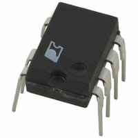
LNK501PN Power Integrations, LNK501PN Datasheet - Page 9

LNK501PN
Manufacturer Part Number
LNK501PN
Description
IC SWIT OCP CV/CC HV 8DIP
Manufacturer
Power Integrations
Series
LinkSwitch®r
Datasheet
1.LNK501PN.pdf
(20 pages)
Specifications of LNK501PN
Output Isolation
Isolated
Frequency Range
26 ~ 46kHz
Voltage - Output
700V
Power (watts)
4W
Operating Temperature
-40°C ~ 150°C
Package / Case
8-DIP (0.300", 7.62mm), 7 Leads
Output Voltage
5.6 V
Input / Supply Voltage (max)
265 VAC
Input / Supply Voltage (min)
85 VAC
Duty Cycle (max)
80 %
Switching Frequency
42 KHz
Supply Current
1.06 mA
Operating Temperature Range
- 40 C to + 150 C
Mounting Style
Through Hole
For Use With
596-1001 - KIT DESIGN ACCELERATOR ADAPTER
Lead Free Status / RoHS Status
Lead free / RoHS Compliant
Other names
596-1031-5
Available stocks
Company
Part Number
Manufacturer
Quantity
Price
Company:
Part Number:
LNK501PN
Manufacturer:
PowerInt
Quantity:
5 700
Part Number:
LNK501PN
Manufacturer:
POWER
Quantity:
20 000
Part Number:
LNK501PN/GN
Manufacturer:
专营POWER
Quantity:
20 000
At very light or no-load, typically less than 2 mA of output current,
the output voltage rises due to leakage inductance peak charging
of the secondary. This voltage rise can be reduced with a small
preload with little change to no-load power consumption.
The output voltage load variation can be improved across the
whole load range by adding an optocoupler and secondary
reference (Figure 6). The secondary reference is designed to only
provide feedback above the normal peak power point voltage
to maintain the correct constant current characteristic.
Component Selection
The schematic shown in Figure 5 outlines the key components
needed for a LinkSwitch supply.
Clamp diode – D1
Diode D1 should be either a fast (t
type (t
recovery types are preferred, being typically lower cost. Slow
diodes are not recommended; they can allow excessive DRAIN
ringing and the LinkSwitch to be reverse biased.
Clamp Capacitor – C2
Capacitor C2 should be a 0.1 µF, 100 V capacitor. Low cost
metallized plastic film types are recommended. The tolerance
of this part has a very minor effect on the output characteristic
so any of the standard ±5%, ±10% or ±20% tolerances are
acceptable. Ceramic capacitors are not recommended. The
common dielectrics used such as Y5U or Z5U are not stable
with voltage or temperature and may cause output instability.
Ceramic capacitors with high stability dielectrics may be used
but are expensive compared to metallized film types.
CONTROL Pin Capacitor – C1
Capacitor C1 is used during start-up to power LinkSwitch and
sets the auto-restart frequency. For designs that have a battery
load this component should have a value of 0.22 µF and for
resistive loads a value of 1 µF. This ensures there is sufficient
time during start-up for the output voltage to reach regulation.
Any capacitor type is acceptable with a voltage rating of
10 V or above.
Feedback Resistor – R1
The value of R1 is selected to give a feedback current into the
CONTROL pin of approximately 2.3 mA at the peak output
power point of the supply. The actual value depends on the V
selected during design. Any 1%, 0.25 W resistor is suitable.
Output Diode – D2
Either PN fast, PN ultra-fast or Schottky diodes can be used
depending on the efficiency target for the supply, Schottky
diodes giving higher efficiency then PN diodes. The diode
voltage rating should be sufficient to withstand the output
voltage plus the input voltage transformed through the turns
rr
<50 ns), with a voltage rating of 600 V or higher. Fast
r r
<250 ns) or ultra-fast
OR
ratio (a typical V
Slow recovery diodes are not recommended (1N400X types).
Output Capacitor – C4
Capacitor C4 should be selected such that its voltage and ripple
current specifications are not exceeded.
LinkSwitch Layout considerations
Primary Side Connections
Since the SOURCE pins in a LinkSwitch supply are switching
nodes, the copper area connected to SOURCE together with C1,
C2 and R1 (Figure 5) should be minimized, within the thermal
contraints of the design, to reduce EMI coupling.
The CONTROL pin capacitor C1 should be located as close as
possible to the SOURCE and CONTROL pins.
To minimize EMI coupling from the switching nodes on the
primary to both the secondary and AC input, the LinkSwitch
should be positioned away from the secondary of the transformer
and AC input.
Routing the primary return trace from the transformer primary
around LinkSwitch and associated components further reduces
coupling.
Y capacitor
If a Y capacitor is required, it should be connected close to the
transformer secondary output return pin(s) and the primary bulk
capacitor negative return. Such placement will maximize the
EMI benefit of the Y capacitor and avoid problems in common-
mode surge testing.
Quick Design Checklist
As with any power supply design, all LinkSwitch designs
should be verified on the bench to make sure that component
specifications are not exceeded under worst case conditions.
Note: In a LinkSwitch circuit, the SOURCE is a switching
node. This should be taken into consideration during testing.
Oscilloscope measurements should be made with probe grounded
to DC voltages such as primary return or DC rail but not to
SOURCE. Power supply input voltage should always be supplied
using an isolation transformer. The following minimum set of
tests is strongly recommended:
1. Maximum drain voltage – Verify that V
2. Maximum drain current – At maximum ambient temperature,
675 V at highest input voltage and peak output power.
maximum input voltage and peak output power, verify drain
current waveforms at start-up for any signs of transformer
saturation and excessive leading edge current spikes.
LinkSwitch has a minimum leading edge blanking time of
OR
of 50 V requires a diode PIV of 50 V).
LNK501
DS
does not exceed
2/05
I
9


