TOP258PN Power Integrations, TOP258PN Datasheet - Page 27
TOP258PN
Manufacturer Part Number
TOP258PN
Description
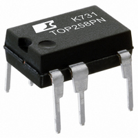
IC OFFLINE SWIT PROG OVP 8DIP
Manufacturer
Power Integrations
Series
TOPSwitch®-HXr
Type
Off Line Switcherr
Datasheet
1.TOP252GN-TL.pdf
(48 pages)
Specifications of TOP258PN
Output Isolation
Isolated
Frequency Range
119 ~ 145kHz
Voltage - Output
700V
Power (watts)
77W
Operating Temperature
-40°C ~ 150°C
Package / Case
8-DIP (0.300", 7.62mm), 7 Leads
Output Voltage
700 V
Input / Supply Voltage (max)
9 V
Input / Supply Voltage (min)
- 0.3 V
Duty Cycle (max)
78 %
Switching Frequency
132 KHz
Operating Temperature Range
- 40 C to + 150 C
Mounting Style
SMD/SMT
Maximum Operating Temperature
+ 150 C
Minimum Operating Temperature
- 40 C
Output Current
6.88 A
Output Power
48 W
For Use With
596-1193 - KIT REF DESIGN TOP HX FOR TOP258
Lead Free Status / RoHS Status
Lead free / RoHS Compliant
Other names
596-1189-5
Available stocks
Company
Part Number
Manufacturer
Quantity
Price
Company:

Part Number:
TOP258PN
Manufacturer:
PowerInt
Quantity:
2 100
Company:
Part Number:
TOP258PN
Manufacturer:
PANASONIC
Quantity:
230
Part Number:
TOP258PN
Manufacturer:
CN/如韵
Quantity:
20 000


Figure 45a. Fixed Frequency Operation Without Jitter.
Figure 45b. TOPSwitch-HX Full Range EMI Scan (132 kHz With Jitter) With
Standby Consumption
Frequency reduction can signifi cantly reduce power loss at light
or no load, especially when a Zener clamp is used. For very
low secondary power consumption, use a TL431 regulator for
feedback control. A typical TOPSwitch-HX circuit automatically
enters MCM mode at no load and the low frequency mode at
light load, which results in extremely low losses under no-load
or standby conditions.
High Power Designs
The TOPSwitch-HX family contains parts that can deliver up to
333 W. High power designs need special considerations.
Guidance for high power designs can be found in the Design
Guide for TOPSwitch-HX (AN-43).
TOPSwitch-HX Layout Considerations
The TOPSwitch-HX has multiple pins and may operate at
high power levels. The following guidelines should be
carefully followed.
www.powerint.com
-10
-10
-20
-10
-10
-20
80
70
60
50
40
30
20
80
70
60
50
40
30
20
0
0
0.15
0.15
Identical Circuitry and Conditions.
TOPSwitch-HX (with jitter)
Frequency (MHz)
Frequency (MHz)
1
1
EN55022B (QP)
EN55022B (AV)
EN55022B (QP)
EN55022B (AV)
10
10
30
30
Primary Side Connections
Use a single point (Kelvin) connection at the negative terminal of
the input fi lter capacitor for the TOPSwitch-HX SOURCE pin
and bias winding return. This improves surge capabilities by
returning surge currents from the bias winding directly to the
input fi lter capacitor. The CONTROL pin bypass capacitor
should be located as close as possible to the SOURCE and
CONTROL pins, and its SOURCE connection trace should not
be shared by the main MOSFET switching currents. All
SOURCE pin referenced components connected to the MULTI-
FUNCTION (M-pin), VOLTAGE MONITOR (V-pin) or EXTERNAL
CURRENT LIMIT (X-pin) pins should also be located closely
between their respective pin and SOURCE. Once again, the
SOURCE connection trace of these components should not be
shared by the main MOSFET switching currents. It is very
critical that SOURCE pin switching currents are returned to the
input capacitor negative terminal through a separate trace that
is not shared by the components connected to CONTROL,
MULTI-FUNCTION, VOLTAGE MONITOR or EXTERNAL
CURRENT LIMIT pins. This is because the SOURCE pin is also
the controller ground reference pin. Any traces to the M, V or X
pins should be kept as short as possible and away from the
DRAIN trace to prevent noise coupling. VOLTAGE MONITOR
resistors (R1 and R2 in Figures 46, 47, 48, R3 and R4 in
Figure 49, and R14 in Figure 50) should be located close to the
M or V pin to minimize the trace length on the M or V pin side.
Resistors connected to the M, V or X pin should be connected
as close to the bulk cap positive terminal as possible while
routing these connections away from the power switching
circuitry. In addition to the 47 μF CONTROL pin capacitor, a
high frequency bypass capacitor in parallel may be used for
better noise immunity. The feedback optocoupler output
should also be located close to the CONTROL and SOURCE
pins of TOPSwitch-HX.
Y-Capacitor
The Y-capacitor should be connected close to the secondary
output return pin(s) and the positive primary DC input pin of the
transformer.
Heat Sinking
The tab of the Y package (TO-220C) and E package (eSIP-7C)
and L package (eSIP-7F) are internally electrically tied to the
SOURCE pin. To avoid circulating currents, a heat sink
attached to the tab should not be electrically tied to any primary
ground/source nodes on the PC board. When using a
P (DIP-8), G (SMD-8) or M (DIP-10) package, a copper area
underneath the package connected to the SOURCE pins will
act as an effective heat sink. On double sided boards, topside
and bottom side areas connected with vias can be used to
increase the effective heat sinking area. In addition, suffi cient
copper area should be provided at the anode and cathode
leads of the output diode(s) for heat sinking. In Figures 46 to 50
a narrow trace is shown between the output rectifi er and output
fi lter capacitor. This trace acts as a thermal relief between the
rectifi er and fi lter capacitor to prevent excessive heating of the
capacitor.
TOP252-262
Rev. F 01/09
27
Related parts for TOP258PN
Image
Part Number
Description
Manufacturer
Datasheet
Request
R

Part Number:
Description:
SOP-16
Manufacturer:
Power Integrations
Datasheet:
Part Number:
Description:
DIP8
Manufacturer:
Power Integrations
Datasheet:
Part Number:
Description:
TO-263
Manufacturer:
Power Integrations
Datasheet:
Part Number:
Description:
TO-263
Manufacturer:
Power Integrations
Datasheet:
Part Number:
Description:
Manufacturer:
Power Integrations
Datasheet: