TOP223YN Power Integrations, TOP223YN Datasheet - Page 4
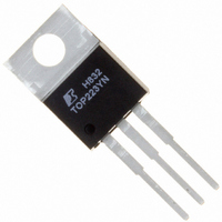
TOP223YN
Manufacturer Part Number
TOP223YN
Description
IC OFFLINE SWIT PWM OCP HV TO220
Manufacturer
Power Integrations
Series
TOPSwitch®-IIr
Type
Off Line Switcherr
Datasheet
1.TOP222GN-TL.pdf
(20 pages)
Specifications of TOP223YN
Output Isolation
Isolated
Frequency Range
90 ~ 110kHz
Voltage - Output
700V
Power (watts)
50W
Operating Temperature
-40°C ~ 150°C
Package / Case
TO-220-3
Output Voltage
5.7 V
Input / Supply Voltage (max)
265 VAC
Input / Supply Voltage (min)
85 VAC
Duty Cycle (max)
70 %
Switching Frequency
100 KHz
Supply Current
1.2 mA
Operating Temperature Range
- 40 C to + 150 C
Mounting Style
Through Hole
Supply Voltage
265VAC
No. Of Pins
3
No. Of Regulated Outputs
1
Filter Terminals
Through Hole
Output Voltage Max
700V
Rohs Compliant
Yes
Operating Temperature Max
150°C
Lead Free Status / RoHS Status
Lead free / RoHS Compliant
Other names
596-1158-5
TOP223YN
TOP223YN
Available stocks
Company
Part Number
Manufacturer
Quantity
Price
Company:

Part Number:
TOP223YN
Manufacturer:
PowerInt
Quantity:
3 250
Part Number:
TOP223YN
Manufacturer:
POWER
Quantity:
20 000


TOPSwitch-II Family Functional Description (cont.)
Control Voltage Supply
CONTROL pin voltage V
controller and driver circuitry. An external bypass capacitor
closely connected between the CONTROL and SOURCE pins
is required to supply the gate drive current. The total amount
of capacitance connected to this pin (C
restart timing as well as control loop compensation. V
regulated in either of two modes of operation. Hysteretic
regulation is used for initial start-up and overload operation.
Shunt regulation is used to separate the duty cycle error signal
from the control circuit supply current. During start-up,
CONTROL pin current is supplied from a high-voltage switched
current source connected internally between the DRAIN and
CONTROL pins. The current source provides sufficient current
to supply the control circuitry as well as charge the total
external capacitance (C
The first time V
current source is turned off and the PWM modulator and output
transistor are activated, as shown in Figure 5(a). During normal
operation (when the output voltage is regulated) feedback
control current supplies the V
regulator keeps V
pin feedback current exceeding the required DC supply current
through the PWM error signal sense resistor R
dynamic impedance of this pin (Z
amplifier when used in a primary feedback configuration. The
dynamic impedance of the CONTROL pin together with the
external resistance and capacitance determines the control loop
compensation of the power system.
If the CONTROL pin total external capacitance (C
discharge to the lower threshold, the output MOSFET is turned
off and the control circuit is placed in a low-current standby
mode. The high-voltage current source turns on and charges the
external capacitance again. Charging current is shown with a
negative polarity and discharging current is shown with a
positive polarity in Figure 6. The hysteretic auto-restart
comparator keeps V
by turning the high-voltage current source on and off as shown
in Figure 5(b). The auto-restart circuit has a divide-by-8
counter which prevents the output MOSFET from turning on
again until eight discharge-charge cycles have elapsed. The
counter effectively limits TOPSwitch power dissipation by
reducing the auto-restart duty cycle to typically 5%. Auto-
restart continues to cycle until output voltage regulation is
again achieved.
Bandgap Reference
All critical TOPSwitch internal voltages are derived from a
temperature-compensated bandgap reference. This reference
is also used to generate a temperature-compensated current
source which is trimmed to accurately set the oscillator frequency
and MOSFET gate drive current.
4
TOP221-227
D
7/01
C
reaches the upper threshold, the high-voltage
C
at typically 5.7 V by shunting CONTROL
C
within a window of typically 4.7 to 5.7 V
T
).
C
is the supply or bias voltage for the
C
supply current. The shunt
C
) sets the gain of the error
T
) also sets the auto-
E
. The low
T
) should
C
is
Oscillator
The internal oscillator linearly charges and discharges the
internal capacitance between two voltage levels to create a
sawtooth waveform for the pulse width modulator. The oscillator
sets the pulse width modulator/current limit latch at the beginning
of each cycle. The nominal frequency of 100 kHz was chosen
to minimize EMI and maximize efficiency in power supply
applications. Trimming of the current reference improves the
frequency accuracy.
Pulse Width Modulator
The pulse width modulator implements a voltage-mode control
loop by driving the output MOSFET with a duty cycle inversely
proportional to the current into the CONTROL pin which
generates a voltage error signal across R
across R
frequency of 7 kHz to reduce the effect of switching noise. The
filtered error signal is compared with the internal oscillator
sawtooth waveform to generate the duty cycle waveform. As
the control current increases, the duty cycle decreases. A clock
signal from the oscillator sets a latch which turns on the output
MOSFET. The pulse width modulator resets the latch, turning
off the output MOSFET. The maximum duty cycle is set by the
symmetry of the internal oscillator. The modulator has a
minimum ON-time to keep the current consumption of the
TOPSwitch independent of the error signal. Note that a minimum
current must be driven into the CONTROL pin before the duty
cycle begins to change.
Gate Driver
The gate driver is designed to turn the output MOSFET on at a
controlled rate to minimize common-mode EMI. The gate drive
current is trimmed for improved accuracy.
Error Amplifier
The shunt regulator can also perform the function of an error
amplifier in primary feedback applications. The shunt regulator
voltage is accurately derived from the temperature compensated
bandgap reference. The gain of the error amplifier is set by the
CONTROL pin dynamic impedance. The CONTROL pin
clamps external circuit signals to the V
CONTROL pin current in excess of the supply current is
separated by the shunt regulator and flows through R
voltage error signal.
Cycle-By-Cycle Current Limit
The cycle by cycle peak drain current limit circuit uses the
output MOSFET ON-resistance as a sense resistor. A current
limit comparator compares the output MOSFET ON-state drain-
source voltage, V
current causes V
the output MOSFET off until the start of the next clock cycle.
The current limit comparator threshold voltage is temperature
E
is filtered by an RC network with a typical corner
DS(ON)
DS(ON)
to exceed the threshold voltage and turns
with a threshold voltage. High drain
C
E
voltage level. The
. The error signal
E
as a
Related parts for TOP223YN
Image
Part Number
Description
Manufacturer
Datasheet
Request
R

Part Number:
Description:
SOP-16
Manufacturer:
Power Integrations
Datasheet:
Part Number:
Description:
DIP8
Manufacturer:
Power Integrations
Datasheet:
Part Number:
Description:
TO-263
Manufacturer:
Power Integrations
Datasheet:
Part Number:
Description:
TO-263
Manufacturer:
Power Integrations
Datasheet:
Part Number:
Description:
Manufacturer:
Power Integrations
Datasheet: