TOP247YN Power Integrations, TOP247YN Datasheet - Page 6
TOP247YN
Manufacturer Part Number
TOP247YN
Description
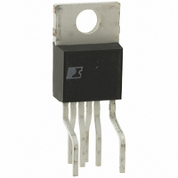
IC OFFLINE SWIT UVLO HV TO220
Manufacturer
Power Integrations
Series
TOPSwitch®-GXr
Type
Off Line Switcherr
Datasheet
1.TOP242GN-TL.pdf
(52 pages)
Specifications of TOP247YN
Output Isolation
Isolated
Frequency Range
66 ~ 132kHz
Voltage - Output
700V
Power (watts)
165W
Operating Temperature
-40°C ~ 150°C
Package / Case
TO-220-7 (Formed Leads), 5 Leads
Output Voltage
12 V
Input / Supply Voltage (max)
265 VAC
Input / Supply Voltage (min)
85 VAC
Duty Cycle (max)
83 %
Switching Frequency
132 KHz
Supply Current
2.2 mA
Operating Temperature Range
- 40 C to + 150 C
Mounting Style
Through Hole
Supply Voltage
265VAC
No. Of Pins
6
No. Of Regulated Outputs
1
Filter Terminals
Through Hole
Output Voltage Max
700V
Rohs Compliant
Yes
On Resistance Rds(on)
1.95ohm
Lead Free Status / RoHS Status
Lead free / RoHS Compliant
Other names
596-1078-5
Available stocks
Company
Part Number
Manufacturer
Quantity
Price
Company:

Part Number:
TOP247YN
Manufacturer:
PowerInt
Quantity:
18 550
Company:
Part Number:
TOP247YN
Manufacturer:
POWER
Quantity:
3 910
Part Number:
TOP247YN
Manufacturer:
POWER
Quantity:
20 000
Part Number:
TOP247YN .
Manufacturer:
POWER
Quantity:
20 000


CONTROL (C) Pin Operation
The CONTROL pin is a low impedance node that is capable
of receiving a combined supply and feedback current. During
normal operation, a shunt regulator is used to separate the
feedback signal from the supply current. CONTROL pin voltage
V
MOSFET gate driver. An external bypass capacitor closely
connected between the CONTROL and SOURCE pins is required
to supply the instantaneous gate drive current. The total amount
of capacitance connected to this pin also sets the auto-restart
timing as well as control loop compensation.
When rectified DC high voltage is applied to the DRAIN
pin during start-up, the MOSFET is initially off, and the
CONTROL pin capacitor is charged through a switched high
voltage current source connected internally between the DRAIN
and CONTROL pins. When the CONTROL pin voltage V
reaches approximately 5.8 V, the control circuitry is activated
and the soft-start begins. The soft-start circuit gradually
increases the duty cycle of the MOSFET from zero to the
maximum value over approximately 10 ms. If no external
feedback/supply current is fed into the CONTROL pin by the
end of the soft-start, the high voltage current source is turned
off and the CONTROL pin will start discharging in response
to the supply current drawn by the control circuitry. If the
power supply is designed properly, and no fault condition
such as open loop or shorted output exists, the feedback loop
will close, providing external CONTROL pin current, before
the CONTROL pin voltage has had a chance to discharge to
the lower threshold voltage of approximately 4.8 V (internal
supply under-voltage lockout threshold). When the externally
fed current charges the CONTROL pin to the shunt regulator
Figure 8. Typical Waveforms for (1) Power Up (2) Normal Operation (3) Auto-Restart (4) Power Down.
C
6
is the supply voltage for the control circuitry including the
TOP242-250
V
V
V
Note: S0 through S7 are the output states of the auto-restart counter
LINE
C
V
DRAIN
0 V
0 V
0 V
0 V
O
11/05
OUT
V
UV
1
S7
S0
2
S1
S2
S6
S7
3
S0
S1
C
S2
voltage of 5.8 V, current in excess of the consumption of the
chip is shunted to SOURCE through resistor R
Figure 2. This current flowing through R
of the power MOSFET to provide closed loop regulation. The
shunt regulator has a finite low output impedance Z
the gain of the error amplifier when used in a primary feedback
configuration. The dynamic impedance Z
pin together with the external CONTROL pin capacitance sets
the dominant pole for the control loop.
When a fault condition such as an open loop or shorted output
prevents the flow of an external current into the CONTROL
pin, the capacitor on the CONTROL pin discharges towards
4.8 V. At 4.8 V, auto-restart is activated which turns the output
MOSFET off and puts the control circuitry in a low current
standby mode. The high-voltage current source turns on and
charges the external capacitance again. A hysteretic internal
supply under-voltage comparator keeps V
of typically 4.8 V to 5.8 V by turning the high-voltage current
source on and off as shown in Figure 8. The auto-restart
circuit has a divide-by-eight counter which prevents the output
MOSFET from turning on again until eight discharge/charge
cycles have elapsed. This is accomplished by enabling the
output MOSFET only when the divide-by-eight counter reaches
full count (S7). The counter effectively limits TOPSwitch-GX
power dissipation by reducing the auto-restart duty cycle
to typically 4%. Auto-restart mode continues until output
voltage regulation is again achieved through closure of the
feedback loop.
Oscillator and Switching Frequency
The internal oscillator linearly charges and discharges an
S6
S7
2
S0
S1
S2
4
S6
E
S7
controls the duty cycle
C
C
S7
of the CONTROL
within a window
E
4.8 V
as shown in
PI-2545-082299
5.8 V
C
that sets
Related parts for TOP247YN
Image
Part Number
Description
Manufacturer
Datasheet
Request
R

Part Number:
Description:
SOP-16
Manufacturer:
Power Integrations
Datasheet:
Part Number:
Description:
DIP8
Manufacturer:
Power Integrations
Datasheet:
Part Number:
Description:
TO-263
Manufacturer:
Power Integrations
Datasheet:
Part Number:
Description:
TO-263
Manufacturer:
Power Integrations
Datasheet:
Part Number:
Description:
Manufacturer:
Power Integrations
Datasheet: