VIPER50-22-E STMicroelectronics, VIPER50-22-E Datasheet
VIPER50-22-E
Specifications of VIPER50-22-E
VIPER50-22-E
Available stocks


Related parts for VIPER50-22-E


VIPER50-22-E Summary of contents
Page 1
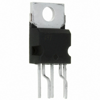
... DS(on) Ω 1.5A 5 PENTAWATT HV Description VIPer50-E, made using VIPower M0 Technology, combines on the same silicon chip a state-of-the- art PWM circuit together with an optimized, high voltage, Vertical Power MOSFET (620V/ 1.5A). Typical applications cover offline power supplies with a secondary power capability of 25W in wide range condition and 50W in single range or with doubler configuration ...
Page 2
... OSC Pin (Oscillator Frequency Typical Circuit . . . . . . . . . . . . . . . . . . . . . . . . . . . . . . . . . . . . . . . . . . . . . . . 10 5 Operation Description . . . . . . . . . . . . . . . . . . . . . . . . . . . . . . . . . . . . . . . . . 11 5.1 Current Mode Topology .11 5.2 Stand-by Mode . . . . . . . . . . . . . . . . . . . . . . . . . . . . . . . . . . . . . . . . . . . . . . . .11 5.3 High Voltage Start-up Current Suorce . . . . . . . . . . . . . . . . . . . . . . . . . . . . . . 12 5.4 Transconductance Error Amplifier . . . . . . . . . . . . . . . . . . . . . . . . . . . . . . . . . 13 5.5 External Clock Synchronization 5.6 Primary Peak Current Limitation . . . . . . . . . . . . . . . . . . . . . . . . . . . . . . . . . . 14 5.7 Over-Temperature Protection . . . . . . . . . . . . . . . . . . . . . . . . . . . . . . . . . . . . 14 5.8 Operation Pictures . . . . . . . . . . . . . . . . . . . . . . . . . . . . . . . . . . . . . . . . . . . . 15 2/29 VIPer50-E ...
Page 3
... VIPer50-E 6 Electrical Over Stress . . . . . . . . . . . . . . . . . . . . . . . . . . . . . . . . . . . . . . . . . 21 6.1 Electrical Over Stress Ruggedness . . . . . . . . . . . . . . . . . . . . . . . . . . . . . . . 21 7 Layout . . . . . . . . . . . . . . . . . . . . . . . . . . . . . . . . . . . . . . . . . . . . . . . . . . . . . . 22 7.1 Layout Considerations . . . . . . . . . . . . . . . . . . . . . . . . . . . . . . . . . . . . . . . . . 22 8 Package Mechanical Data . . . . . . . . . . . . . . . . . . . . . . . . . . . . . . . . . . . . . . 23 9 Order Codes . . . . . . . . . . . . . . . . . . . . . . . . . . . . . . . . . . . . . . . . . . . . . . . . . 27 10 Revision history . . . . . . . . . . . . . . . . . . . . . . . . . . . . . . . . . . . . . . . . . . . . . . 28 3/29 ...
Page 4
... Avalanche Drain-Source Current, Repetitive or Not Repetitive D(AR 100°C; Pulse width limited Power Dissipation at T TOT T Junction Operating Temperature J T Storage Temperature STG 4/29 Parameter = 25 to 125°C) J max; δ < 1 25ºC C VIPer50-E Value Unit –0.3 to 620 V Internally limited ±2 mA 4000 V 1 ° ...
Page 5
... VIPer50-E 1.2 Electrical Characteristics T = 25° 13V, unless otherwise specified J DD Table 2. Power Section Symbol Parameter BV Drain-Source Voltage DS I Off-State Drain DSS Current R Static Drain-Source DS(on) On Resistance t Fall Time f t Rise Time r C Output Capacitance oss (1) On Inductive Load, Clamped. Table 3. ...
Page 6
... DD V =2.5V; V =12V COMP DD Test Conditions‘ COMP I = 10mA DPEAK V = 12V; COMP pin open 0.5A D Test Conditions‘ (see Figure 8) (see Figure 8) (see Figure 8) (see Figure 8) VIPer50-E Min Typ Max Unit 12 150 KHz 1.1 1.5 1.9 mA/V 0.2 V 4.5 V -600 µ ...
Page 7
... VIPer50-E 2 Thermal Data Table 8. Thermal data Symbol R Thermal Resistance Junction-case thJC R Thermal Resistance Ambient-case thJA Parameter Max Max 2 Thermal Data PENTAWATT HV Unit °C/W 1.9 °C/W 60 7/29 ...
Page 8
... COMP pin is shorted to DD voltage, which cannot overpass 13V. The output voltage DD VIPer50-E goes below DD at 13V. For secondary regulation, a pin by transformer design, in order to DD ...
Page 9
... VIPer50-E 3.5 OSC Pin (Oscillator Frequency network must be connected on that to define the switching frequency. Note that t t despite the connection of R from 8V to 15V. It provides also a synchronisation capability, when connected to an external frequency source. Figure 1. Connection Diagrams (Top View) PENTAWATT HV Figure 2. ...
Page 10
... Figure 4. Offline Power Supply With Optocoupler Feedback F1 TR2 10/29 BR1 VDD DRAIN - OSC + 13V COMP SOURCE C6 C11 R3 BR1 VDD DRAIN - U1 OSC VIPer100 + 13V COMP SOURCE C6 C11 R3 TR1 C10 VIPer50 FC00301 TR1 D2 L2 +Vcc C7 C9 GND C10 R6 ISO1 FC00091 VIPer50-E +Vcc GND ...
Page 11
... Current Mode Topology: The current mode control method, like the one integrated in the VIPer50-E, uses two control loops - an inner current control loop and an outer loop for voltage control. When the Power MOSFET output transistor is on, the inductor current (primary side of the transformer) is monitored with a SenseFET technique and converted into a voltage V current ...
Page 12
... The equivalent switching frequency is also lower than the normal one, leading to a reduced consumption on the input main supply lines. This mode of operation allows the VIPer50-E to meet the new German "Blue Angel" Norm with less than 1W total power consumption for the system when working in stand-by mode ...
Page 13
... Figure 18) shutdown. Once the "Shutdown" signal has been activated, the device remains in the Off state until the input voltage is removed. 5.4 Transconductance Error Amplifier The VIPer50-E includes a transconductance error amplifier. Transconductance Gm is the change in output current (I ∂l COMP G = ------------------ - ∂ ...
Page 14
... The device is automatically restarted when the junction temperature decreases to the restart temperature threshold that is typically 40ºC below the shutdown value 14/29 Figure 22 . The circuit based on Q1, R – 0 the range of 220KΩ VIPer50-E and R clamps the voltage (see Figure 13) ...
Page 15
... VIPer50-E 5.8 Operation Pictures Figure 5. V Regulation Point Slope = A/V COM COM PLO V DDreg Figure 7. Transition Time I D 10% Ipeak Figure 9. Breakdown Voltage vs. Temperature Figure 10. Typical Frequency Variation 1.15 BV DSS (Normalized) 1.1 1. Temperature (°C) Figure FC00150 Figure FC00160 ...
Page 16
... Operation Description Figure 11. Behaviour of the high voltage current source at start-up VDD VDDon VDDoff t Figure 12. Start-Up Waveforms 16/ VDD VDD Ref. UNDERVOLTAGE Auxiliary primary LOCK OUT LOGIC winding VIPer50 Start up duty cycle ~ 12% VIPer50-E DRAIN 3 mA SOURCE FC00320 ...
Page 17
... VIPer50-E Figure 13. Over-temperature Protection Operation Description 17/29 ...
Page 18
... Ct = 4.7 nF 200 100 18/29 For R CLK FC 00050 Forbidden area Ct(nF) = Forbidden area 40kHz Oscillator frequency vs Rt and 2 (kΩ) ≤ 40KHz > 1.2kΩ and 2.3 550 ⋅ ---------- - 1 – ------------------- - ⎛ ⎞ – 150 ⎠ 880 Fsw(kHz) Fsw FC00030 FC00030 VIPer50-E ...
Page 19
... VIPer50-E Figure 15. Error Amplifier frequency Response 60 RCOMP = +∞ RCOMP = 270k 40 RCOMP = 82k RCOMP = 27k RCOMP = 12k 20 0 (20) 0.001 Figure 16. Error Amplifier Phase Response 200 150 100 50 0 (50) 0.001 0.01 0 Frequency (kHz) 0.01 0 Frequency (kHz) 5 Operation Description FC00200 100 1,000 FC00210 RCOMP = +∞ ...
Page 20
... Figure 21. External Clock Sinchronisation OSC 10 kΩ 20/ AUXILIARY WINDING R2 Shutdown + C2 FC00331 Figure 20. Slope Compensation DRAIN FC00351 Figure 22. Current Limitation Circuit Example VIPer50 VDD DRAIN - + 13V COMP SOURCE FC00370 VIPer50-E VIPer50 R1 VDD Q2 - OSC + 13V COMP SOURCE FC00340 R 1 VIPer5 RAIN - 13V 00361 ...
Page 21
... VIPer50-E 6 Electrical Over Stress 6.1 Electrical Over Stress Ruggedness The VIPer may be submitted to electrical over-stress, caused by violent input voltage surges or lightning. Following the Layout Considerations is sufficient to prevent catastrophic damages most of the time. However in some cases, the voltage surges coupled through the transformer ...
Page 22
... Signal components C2, ISO1, C3, and C4 are using a dedicated track connected directly to the power source of the device. Figure 24. Recommended Layout R1 C1 OSC From input diodes bridge U1 VIPerXX0 C2 22/29 (see Figure D2 VDD DRAIN - C5 + 13V COMP SOURCE R2 C3 ISO1 C4 VIPer50-E 24 secondary C7 filtering and load C6 FC00500 ...
Page 23
... VIPer50-E 8 Package Mechanical Data In order to meet environmental requirements, ST offers these devices in ECOPACK packages. These packages have a Lead-free second level interconnect . The category of second Level Interconnect is marked on the package and on the inner box label, in compliance with JEDEC Standard JESD97. The maximum ratings related to soldering conditions are also marked on the inner box label ...
Page 24
... VIPer50-E inch Min. Typ. Max. 0.169 0.189 0.046 0.054 0.094 0.11 0.014 0.022 0.024 0.031 0.193 0.205 0.295 0.307 0.366 0.382 ...
Page 25
... VIPer50-E Pentawatt HV 022Y ( Vertical High Pitch ) Mechanical Data Dim Min. A 4.30 C 1.17 D 2.40 E 0.35 F 0.60 G1 4.91 G2 7. 10.05 L 16.42 L1 14.60 L3 20.52 L5 2.60 L6 15.10 L7 6.00 M 2. Diam 3.65 mm. Typ. Maw. 4.80 1.37 2.80 0.55 0.80 5.21 7.80 9.70 10.40 10.40 17 ...
Page 26
... Package Mechanical Data Figure 25. Pentawatt HV Tube Shipment ( no suffix ) 26/29 Base Q.ty 50 1000 Bulk Q.ty Tube length ( ± 0.5 ) 532 33 ± 0 All dimensions are in mm. VIPer50-E ...
Page 27
... VIPer50-E 9 Order Codes PENTAWATT HV VIPer50-E 9 Order Codes PENTAWATT HV (022Y) VIPer50-22-E 27/29 ...
Page 28
... Revision history 10 Revision history Date Revision 26-Sep-2005 1 28/29 Initial release. VIPer50-E Changes ...
Page 29
... VIPer50-E Information furnished is believed to be accurate and reliable. However, STMicroelectronics assumes no responsibility for the consequences of use of such information nor for any infringement of patents or other rights of third parties which may result from its use. No license is granted by implication or otherwise under any patent or patent rights of STMicroelectronics. Specifications mentioned in this publication are subject to change without notice ...